


 The Chemical Connection Onshoring PCB Production—Daunting but Certainly Possible
 It’s Only Common Sense: The Phone Is Still Mightier Than the Keyboard


New Semiconducting Crystal Rivals Diamond for Heat Conductivity
July 12, 2018 | University of Texas at AustinEstimated reading time: 3 minutes
The need for faster and smaller electronics has resulted in microelectronic components that produce progressively more heat. Thus, heat dissipation is an important issue, and one solution for cooling is to develop novel semiconducting materials with high thermal conductivity.
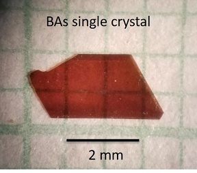
Fragment of boron arsenide crystal under a microscope.Engineers and scientists have long known that diamond is the best material for conducting heat, but it has its drawbacks — the most obvious being that it is quite costly. It is also an electrical insulator. In addition, when paired with a semiconductor device, diamond expands at a different rate than the device does when it is heated.
Now, a group of engineers from the Cockrell School of Engineering at The University of Texas at Austin, along with research partners across Texas and the U.S., has found a crystal material from two relatively common elements — boron and arsenic — that demonstrates far higher thermal conductivity than any other semiconductors and metals currently in use, such as silicon, silicon carbide, copper and silver.
The team’s discovery, which was published in the July 5 issue of Science, could offer a more viable alternative to diamond for addressing a range of technological challenges, including cooling electronic devices and nanodevices.
Thermal conductivity is measured in the unit of Wm-1K-1, used to denote the amount of heat flux that can pass through a material that is 1 meter long when the temperature difference from one side to the other is 1 Kelvin. The boron arsenide crystals have a conductivity about 1,000 Wm-1K-1 at room temperature, the researchers reported.
Copper, by comparison, has a conductivity of about 400 Wm-1K-1, and diamond has a reported thermal conductivity of 2,000 Wm-1K-1 at room temperature.
The crystals were grown by a team led by professor Zhifeng Ren at the University of Houston. The high thermal conductivity was validated by the Cockrell School’s team and another team led by professor Gang Chen at MIT. The UT Austin team includes post-doc fellows Xi Chen and Jaehyun Kim, graduate students Sean Sullivan and Yuanyuan Zhou and professors Jianshi Zhou and Li Shi from the Cockrell School’s Department of Mechanical Engineering and Texas Materials Institute.
It is difficult to measure the thermal conductivity accurately when the value is high, because the temperature gradient is very small. When the boron arsenide crystals were measured using a tightly focused laser beam, the measured thermal conductivity values varied across different locations of the same sample. To address the problem, the UT Austin team devised two different sensitive methods to measure the average thermal conductivity of the entire bulk crystal.
“With these methods, we have confirmed that the average bulk thermal conductivity reaches impressive levels at room temperature,” said Chen, one of the post-docs on the project. “The obtained temperature dependence of thermal conductivity also reveals unique thermal transport mechanisms.”
Team member Sean Sullivan, a Ph.D. candidate in UT materials science and engineering said the unique thing about boron arsenide is that it is the only semiconductor that we know of with high thermal conductivity.
“It breaks long-held criteria thought to be critical for developing materials with superior thermal transport characteristics,” Sullivan said.
The experiments have been motivated by a theoretical prediction from professor David Broido at Boston College along with Lucas Lindsay and Tom Reinecke at the Naval Research Lab. The team’s discovery is an important step toward future applications and uses of boron arsenide.
The next step, said the Cockrell School’s Li Shi, will be “to explore device technologies with the boron arsenide bulk crystals.”
The project was funded by the U.S. Navy’s Multidisciplinary University Research Initiative (MURI). The MURI team is led by Shi and includes researchers from the University of Houston, Boston College, UT Austin, MIT, the University of Illinois Urbana-Champaign and the University of California, Los Angeles.
Share on:


Testimonial
"Your magazines are a great platform for people to exchange knowledge. Thank you for the work that you do."
Simon Khesin - Schmoll MaschinenSuggested Items
Episode 6 of Ultra HDI Podcast Series Explores Copper-filled Microvias in Advanced PCB Design and Fabrication
10/15/2025 | I-Connect007I-Connect007 has released Episode 6 of its acclaimed On the Line with... American Standard Circuits: Ultra High Density Interconnect (UHDI) podcast series. In this episode, “Copper Filling of Vias,” host Nolan Johnson once again welcomes John Johnson, Director of Quality and Advanced Technology at American Standard Circuits, for a deep dive into the pros and cons of copper plating microvias—from both the fabricator’s and designer’s perspectives.
Nolan’s Notes: Tariffs, Technologies, and Optimization
10/01/2025 | Nolan Johnson -- Column: Nolan's NotesLast month, SMT007 Magazine spotlighted India, and boy, did we pick a good time to do so. Tariff and trade news involving India was breaking like a storm surge. The U.S. tariffs shifted India from one of the most favorable trade agreements to the least favorable. Electronics continue to be exempt for the time being, but lest you think that we’re free and clear because we manufacture electronics, steel and aluminum are specifically called out at the 50% tariff levels.
MacDermid Alpha & Graphic PLC Lead UK’s First Horizontal Electroless Copper Installation
09/30/2025 | MacDermid Alpha & Graphic PLCMacDermid Alpha Electronics Solutions, a leading supplier of integrated materials and chemistries to the electronics industry, is proud to support Graphic PLC, a Somacis company, with the installation of the first horizontal electroless copper metallization process in the UK.
Electrodeposited Copper Foils Market to Grow by $11.7 Billion Over 2025-2032
09/18/2025 | Globe NewswireThe global electrodeposited copper foils market is poised for dynamic growth, driven by the rising adoption in advanced electronics and renewable energy storage solutions.
MacDermid Alpha Showcases Advanced Interconnect Solutions at PCIM Asia 2025
09/18/2025 | MacDermid Alpha Electronics SolutionsMacDermid Alpha Electronic Solutions, a global leader in materials for power electronics and semiconductor assembly, will showcase its latest interconnect innovations in electronic interconnect materials at PCIM Asia 2025, held from September 24 to 26 at the Shanghai New International Expo Centre, Booth N5-E30