


 The Chemical Connection Onshoring PCB Production—Daunting but Certainly Possible
 It’s Only Common Sense: The Phone Is Still Mightier Than the Keyboard


Researchers Improve Conductive Property of Graphene, Advancing Promise of Solar Technology
July 12, 2018 | The University of KansasEstimated reading time: 4 minutes
In 2010, the Nobel Prize in Physics went to the discoverers of graphene. A single layer of carbon atoms, graphene possesses properties that are ideal for a host of applications. Among researchers, graphene has been the hottest material for a decade. In 2017 alone, more than 30,000 research papers on graphene were published worldwide.
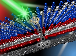
Image: Researchers from the University of Kansas have connected a graphene layer with two other atomic layers (molybdenum diselenide and tungsten disulfide), thereby extending the lifetime of excited electrons in graphene by several hundred times. Credit: Matthew Bellus.
Now, two researchers from the University of Kansas, Professor Hui Zhao and graduate student Samuel Lane, both of the Department of Physics & Astronomy, have connected a graphene layer with two other atomic layers (molybdenum diselenide and tungsten disulfide) thereby extending the lifetime of excited electrons in graphene by several hundred times. The finding will be published on Nano Futures, a newly launched and highly selective journal.
The work at KU may speed development of ultrathin and flexible solar cells with high efficiency.
For electronic and optoelectronic applications, graphene has excellent charge transport property. According to the researchers, electrons move in graphene at a speed of 1/30 of the speed of light — much faster than other materials. This might suggest that graphene can be used for solar cells, which convert energy from sunlight to electricity. But graphene has a major drawback that hinders such applications – its ultrashort lifetime of excited electrons (that is, the time an electron stays mobile) of only about one picosecond (one-millionth of one-millionth of a second, or 10-12 second).
“These excited electrons are like students who stand up from their seats — after an energy drink, for example, which activates students like sunlight activates electrons,” Zhao said. “The energized students move freely in the classroom — like human electric current.”
The KU researcher said one of the biggest challenges to achieving high efficiency in solar cells with graphene as the working material is that liberated electrons — or, the standing students — have a strong tendency to losing their energy and become immobile, like students sitting back down.
“The number of electrons, or students from our example, who can contribute to the current is determined by the average time they can stay mobile after they are liberated by light,” Zhao said. “In graphene, an electron stays free for only one picosecond. This is too short for accumulating a large number of mobile electrons. This is an intrinsic property of graphene and has been a big limiting factor for applying this material in photovoltaic or photo-sensing devices. In other words, although electrons in graphene can become mobile by light excitation and can move quickly, they only stay mobile too short a time to contribute to electricity.”
In their new paper, Zhao and Lane report this issue could be solved by using the so-called van der Waals materials. The principle of their approach is rather simple to understand.
“We basically took the chairs away from the standing students so that they have nowhere to sit,” Zhao said. “This forces the electrons to stay mobile for a time that is several hundred times longer than before.”
To achieve this goal, working in KU’s Ultrafast Laser Lab, they designed a tri-layer material by putting single layers of MoSe2, WS2 and graphene on top of each other.
“We can think of the MoSe2 and graphene layers as two classrooms full of students all sitting, while the middle WS2 layer acts as a hallway separating the two rooms,” Zhao said. “When light strikes the sample, some of the electrons in MoSe2 are liberated. They are allowed to go across the WS2-layer hallway to enter the other room, which is graphene. However, the hallway is carefully designed so that the electrons have to leave their seats in MoSe2. Once in graphene, they have no choice but to stay mobile and hence contribute to electric currents, because their seats are no longer available to them.”
To demonstrate that the idea works, the KU researchers used an ultrashort laser pulse (0.1 picosecond) to liberate some of the electrons in MoSe2. By using another ultrashort laser pulse, they were able to monitor these electrons as they move to graphene. They found that these electrons move through the “hallway” in about 0.5 picosecond on average. They then stay mobile for about 400 picoseconds — a 400-fold improvement than a single layer of graphene, which they also measured in the same study.
The researchers also confirm “seats” left in MoSe2 also stay unoccupied for the same amount of time. In the classical world, these seats should stay empty forever. In quantum mechanics, however, the electrons “tunnel” back to these seats. The researchers propose this process determined the lifetime of the mobile electrons. So, by choosing different “hallway” layers, this time can be controlled for various applications.
The research was funded by National Science Foundation. Lane is supported by Self Graduate Fellowship.
Share on:


Testimonial
"In a year when every marketing dollar mattered, I chose to keep I-Connect007 in our 2025 plan. Their commitment to high-quality, insightful content aligns with Koh Young’s values and helps readers navigate a changing industry. "
Brent Fischthal - Koh YoungSuggested Items
The Marketing Minute: Marketing With Layers
10/15/2025 | Brittany Martin -- Column: The Marketing MinuteMarketing to a technical audience is like crafting a multilayer board: Each layer serves a purpose, from the surface story to the buried detail that keeps everything connected. At I-Connect007, we’ve learned that the best marketing campaigns aren’t built linearly; they’re layered. A campaign might start with a highly technical resource, such as an in-depth article, a white paper, or a podcast featuring an engineer delving into the details of a process. That’s the foundation, the substance that earns credibility.
EDADOC Ushers in a New Era of Robotics Innovation
10/07/2025 | Edy Yu, Editor-in-Chief, ECIOOn Sept. 11, Shanghai Zhiyuan Technology Co., Ltd. (MScape) made a stunning debut at Shanghai’s 2025 Fourth North Bund Cybersecurity Forum and Cyber Intelligence Security Frontier Technology and Equipment Exhibition. The company presented the world’s first Dvorak super heterogeneous architecture and the Zhijing T-series-embodied intelligence (robotics) edge computing power platform. This has been a game-changer in the cybersecurity technology field, filling the gap in the domestic robotics core computing power platform.
Connect the Dots: Evolution of PCB Manufacturing—Lamination
10/02/2025 | Matt Stevenson -- Column: Connect the DotsWhen I wrote The Printed Circuit Designer's Guide to...™ Designing for Reality, it was not a one-and-done effort. Technology is advancing rapidly. Designing for the reality of PCB manufacturing will continue to evolve. That’s why I encourage designers to stay on top of the tools and processes used during production, to ensure their designs capitalize on the capabilities of their manufacturing partner.
Driving Innovation: Mastering Panel Warpage
09/23/2025 | Simon Khesin -- Column: Driving InnovationDuring the complex and multi-step process of PCB fabrication, a panel's flatness is constantly at risk. A host of factors can introduce warpage, bending, and unevenness, presenting a fundamental challenge to achieving high-precision results. This deformation (sometimes referred to as “bow and twist”), even on a microscopic scale, can lead to critical defects during subsequent stages, such as component surface mounting (e.g., tombstoning, solder opens) and the PCB's long-term functional reliability.
Beyond Design: Slaying Signal Integrity Villains
09/17/2025 | Barry Olney -- Column: Beyond DesignHigh-speed PCB design is a balancing act, where subtle oversights can develop into major signal integrity nightmares. Some culprits lie dormant during early validation, only to reveal themselves later through workflow disruptions and elusive performance bottlenecks. Take crosstalk, for example. What begins as a stray signal coupling between traces can ripple through the design, ultimately destabilizing the power distribution network. Each of these troublemakers operates with signature tactics, but they also have well-known vulnerabilities.