


 The Chemical Connection Onshoring PCB Production—Daunting but Certainly Possible
 It’s Only Common Sense: The Phone Is Still Mightier Than the Keyboard


Smallest-Ever Magnetic Vortexes Mark Step Toward New Digital Memory
July 12, 2018 | University of Nebraska-LincolnEstimated reading time: 3 minutes
By twisting magnetism into record-small spirals, University of Nebraska-Lincoln physicists are speeding efforts to turn the digital equivalent of memory lane into a memory racetrack that could save energy and space in next-generation electronics.
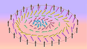
Magnetic materials contain atoms that act like miniature versions of a classic bar magnet, with each featuring a north and south pole. In the materials that exhibit the strongest magnetic fields – the so-called ferromagnets that transform a refrigerator into a photo gallery, for instance – the poles of those atoms all point in the same direction.
But that orderly arrangement can get disrupted by a skyrmion (SKUR’-mee-ahn): a set of atoms whose poles tilt further and further away from the magnetic axis as they approach the skyrmion’s center, with the atom at its core pointing in the opposite direction of that axis.
Researchers had previously created skyrmions with a diameter of about 50 nanometers – roughly 2,000 times thinner than a human hair – in a ferromagnetic material called manganese monosilicide. But a new study led by Nebraska’s David Sellmyer and Balamurugan Balasubramanian has reported the formation of skyrmions just 13 nanometers wide – what seems to be the smallest possible size in the material.
That miniaturization matters, Sellmyer said, if the “interesting magnetic structures” are to fulfill their promise as a next-generation form of digital memory.
“One of the biggest limitations has been the diameter of these things,” said Sellmyer, George Holmes University Distinguished Professor of physics and astronomy. “This discovery is an important step toward exploiting them for real-world applications.”
Digital data storage traditionally exists as separate batches of negatively and positively polarized atoms that represent the 1s and 0s, or bits, of binary code. Because creating and moving a skyrmion demands far less energy than aligning those polarized groups of atoms, researchers see the magnetic spiral as an appealing alternative for digital storage. Under that scenario, the different magnetic signatures produced in the presence and absence of skyrmions would represent the binary bits of data.
“In the past several decades, the density of data storage has gone through the roof,” said Sellmyer, who directs the Nebraska Center for Materials and Nanoscience. “Places all over the country are building these cloud-storage sites. The amount of information that’s getting stored – and the power consumed by these data centers – is getting so high that you practically have to imagine a power plant next to them. So we need faster and much lower-energy data storage.”
Before that can happen, Sellmyer said, researchers need to shrink skyrmions down to a scale that at least rivals existing digital memory formats. Though 13 nanometers is plenty small, the team managed to create such a tiny skyrmion only at extremely low temperatures – minus-382 degrees Fahrenheit being the highest. Finding a method or material that can support minuscule skyrmions at room temperature remains a major goal, he said.
Achieving the feat would also allow researchers to experiment with memory racetracks: nanoscopic stripes that could transport the magnetic vortexes from one group of atoms to another when propelled by an electric current. By bringing those bits to a data reader/writer rather than vice versa, racetrack designs could increase processing speeds and extend the life spans of hard drives.
“A (conventional) hard drive has a disc whirling around with many moving parts, and there are crashes,” Sellmyer said. “This new kind of racetrack-based technology will be a big improvement in that components are not going to wear out, and you use less power.
“A lot of work has to be done in terms of seeing whether one could make, for example, a 20-nanometer-wide stripe and move the skyrmions along it. But that’s the overarching goal of this work.”
The team detailed its findings in the journal Nanoscale, which highlighted the research on its back cover. Sellmyer and Balasubramanian authored the study with Ralph Skomski and Shah Valloppilly of the Nebraska Center for Materials and Nanoscience, along with Bhaskar Das, a doctoral alumnus of Nebraska now at the Ames Laboratory; Pinaki Mukherjee, a former Nebraska postdoctoral researcher now at Rutgers University; and George Hadjipanayis from the University of Delaware.
The U.S. Department of Energy, National Science Foundation and Nebraska Research Initiative supported the team’s work.
Share on:


Testimonial
"The I-Connect007 team is outstanding—kind, responsive, and a true marketing partner. Their design team created fresh, eye-catching ads, and their editorial support polished our content to let our brand shine. Thank you all! "
Sweeney Ng - CEE PCBSuggested Items
ITW EAE Despatch Ovens Now Support ASTM 5423 Testing
10/15/2025 | ITW EAEAs the demand for high-performance electrical insulation materials continues to grow—driven by the rapid expansion of electric vehicles (EVs) and energy storage systems—thermal processing has become a critical step in material development.
Beyond Thermal Conductivity: Exploring Polymer-based TIM Strategies for High-power-density Electronics
10/13/2025 | Padmanabha Shakthivelu and Nico Bruijnis, MacDermid Alpha Electronics SolutionsAs power density and thermal loads continue to increase, effective thermal management becomes increasingly important. Rapid and efficient heat transfer from power semiconductor chip packages is essential for achieving optimal performance and ensuring long-term reliability of temperature-sensitive components. This is particularly crucial in power systems that support advanced applications such as green energy generation, electric vehicles, aerospace, and defense, along with high-speed computing for data centers and artificial intelligence (AI).
Is Glass Finally Coming of Age?
10/13/2025 | Nolan Johnson, I-Connect007Substrates, by definition, form the base of all electronic devices. Whether discussing silicon wafers for semiconductors, glass-and-epoxy materials in printed circuits, or the base of choice for interposers, all these materials function as substrates. While other substrates have come and gone, silicon and FR-4 have remained the de facto standards for the industry.
Creative Materials to Showcase Innovative Functional Inks for Medical Devices at COMPAMED 2025
10/09/2025 | Creative Materials, Inc.Creative Materials, a leading manufacturer of high-performance functional inks and coatings, is pleased to announce its participation in COMPAMED 2025, taking place November 17–20 in Düsseldorf, Germany.
Jiva Leading the Charge Toward Sustainable Innovation
09/30/2025 | Marcy LaRont, PCB007 MagazineEnvironmental sustainability in business—product circularity—is a high priority these days. “Circularity,” the term meant to replace “recycling,” in its simplest definition, describes a full circle life for electronic products and all their elements. The result is re-use or a near-complete reintroduction of the base materials back into the supply chain, leaving very little left for waste. For what cannot be reused productively, the ultimate hope is to have better, less harmful means of disposal and/or materials that can seamlessly and harmlessly decompose and integrate back into the natural environment. That is where Jiva and Soluboard come in.