


 The Chemical Connection Onshoring PCB Production—Daunting but Certainly Possible
 It’s Only Common Sense: The Phone Is Still Mightier Than the Keyboard


Electrical Contact to Molecules in Semiconductor Structures Established for the First Time
July 16, 2018 | University of BaselEstimated reading time: 2 minutes
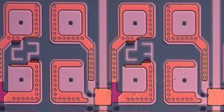
Electrical circuits are constantly being scaled down and extended with specific functions. A new method now allows electrical contact to be established with simple molecules on a conventional silicon chip. The technique promises to bring advances in sensor technology and medicine, as reported in the journal Nature by chemists from the University of Basel and researchers from IBM Research−Zurich in Rüschlikon.
To further develop semiconductor technology, the field of molecular electronics is seeking to manufacture circuit components from individual molecules instead of silicon. Because of their unique electronic properties, molecules are suited to applications that cannot be implemented using conventional silicon technology. However, this requires reliable and inexpensive methods for creating electrical contacts at the two ends of a molecule.
The ability to produce thousands of elements
Researchers from the University of Basel and IBM Research−Zurich have now developed a technique that allows electrical contact to individual molecules to be established. Thousands of stable metal-molecule-metal components can be produced simultaneously by depositing a film of nanoparticles onto the molecules, without compromising the properties of the molecules. This approach was demonstrated using alkane-dithiol compounds, which are made up of carbon, hydrogen, and sulfur.
The researchers used a type of sandwich construction in which an interlayer of molecules is brought into contact with metallic electrodes from above and below. The lower electrode consists of a layer of platinum, which is coated with a layer of non-conducting material. Tiny pores are then etched into this layer to produce arbitrary patterns of compartments of different sizes, inside which there is an electrical contact with the platinum electrode.
Self-assembled monolayers
The researchers then took advantage of the ability of certain molecules to self-assemble. Onto the pattern of pores, they applied a solution containing alkane-dithiol molecules, which self-assemble into the pores, forminga densely packed monolayer film. Within this film, the individual molecules exhibit a regular arrangement and an electrical connection with the lower platinum electrode. Electrical contact with the molecular layer is established via an upper electrode made of gold nanoparticles.
The new technique largely resolves the issues that previously hampered the creation of electrical contacts to molecules - such as high contact resistance or short circuits by filaments penetrating the film. Building blocks fabricated by this method can be operated under standard conditions and provide long-term stability. Moreover, the method can be applied to a variety of other molecular systems and opens up new avenues for integrating molecular compounds into solid-state devices. Its applications could include new types of instruments in the fields of sensor technology and medicine.
"Our approach will help speed up the development of chemically fabricated and controllable electronic and sensor components," says Professor Marcel Mayor of the Department of Chemistry at the University of Basel. The project received significant funding from the National Center of Competence in Research (NCCR) for Molecular Systems Engineering, in which the University of Basel and ETH Zurich are leading houses.
Share on:


Testimonial
"The I-Connect007 team is outstanding—kind, responsive, and a true marketing partner. Their design team created fresh, eye-catching ads, and their editorial support polished our content to let our brand shine. Thank you all! "
Sweeney Ng - CEE PCBSuggested Items
Circus SE Set for High-Volume Market Entry in the Defense Sector
10/17/2025 | BUSINESS WIRECircus SE a global technology leader in AI robotics for autonomous nutrition systems and troop supply, is expanding its global production network as part of its high-volume market entry into the defense sector.
China Expands Rare Earth Export Restrictions, Tightening Grip on Global Supply Chains
10/16/2025 | I-Connect007 Editorial TeamChina sharply expanded its rare earth export restrictions on Oct. 9, adding additional elements and refining technologies to its control list while imposing stricter rules on foreign users in the defense and semiconductor industries.
SAMI Advanced Electronics Company Launches “Remal” Computer Manufacturing Project in Partnership with HP and Foxconn
10/15/2025 | SAMI-AECSAMI Advanced Electronics Company (SAMI-AEC), a wholly owned subsidiary of Saudi Arabian Military Industries (SAMI), proudly announced the launch of the “Remal” project for computer manufacturing, in strategic partnership with HP and Foxconn.
The Right Approach: Electro-Tek—A Williams Family Legacy, Part 1
10/15/2025 | Steve Williams -- Column: The Right ApproachThere is no bronze bust in the lobby or portrait in the conference room of Electro-Tek's founder—my Dad, Charles “Chuck” Williams—so with the facility closing last year after 56 years, I feel it is time to tell the story. Chuck Williams founded Electro-Tek in 1968 in our basement, eventually moving into the second floor of an old 1913 building in downtown Milwaukee that is still standing (the first of three eventual facilities).
LPKF Joins productronica’s 50th Anniversary, Showcasing Laser Technology for Electronics Manufacturing
10/10/2025 | LPKF Laser & ElectronicsLPKF Laser & Electronics invites visitors to productronica 2025 in Munich from November 18 to 21. At booth 305 in hall B2, the company will present its portfolio of modern laser technologies for the electronics industry live – from prototyping systems and high-performance depaneling to laser plastic welding for electronic housings and thin glass processing for advanced packaging.