


 The Chemical Connection Onshoring PCB Production—Daunting but Certainly Possible
 It’s Only Common Sense: The Phone Is Still Mightier Than the Keyboard


A Silicon-Nanoparticle Photonic Waveguide
July 16, 2018 | A*STAREstimated reading time: 2 minutes
A new way to efficiently guide light at tiny scales has been demonstrated by an all-A*STAR team. Their method, which involves lining up silicon nanoparticles, is promising for applications such as light-based integrated circuits, biosensors and quantum communications.
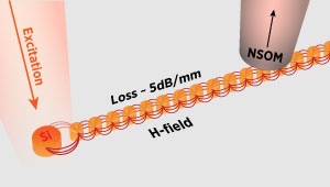
Image caption: Near-field scanning optical microscope (NSOM) measurements have shown that cylindrical silicon nanoparticles arranged in a line can transport light with low loss due to magnetic-field (H-field) resonances between them.
Transporting light on small scales is critical for many applications and is commonly performed using rectangular silicon waveguides — the optical circuit equivalent to wires in electronic circuits. To further shrink devices, metallic nanoparticles have been explored as an alternative, but while they are very good at confining light to small scales, they tend to leak a lot of the light.
Now, Reuben Bakker, Arseniy Kuznetsov and their colleagues at the A*STAR Data Storage Institute have come up with a more efficient method that involves a string of cylindrical silicon nanoparticles. The first nanoparticle is excited using light and then a near-field scanning optical microscope measures the light that reaches another nanoparticle further down the line (see image). When they did this, the team found that the fall in the light intensity was low.
“This is the first experimental demonstration that shows coupled resonators can very efficiently guide light at strongly sub-wavelength dimensions and over lengths of several hundred micrometers,” says Kuznetsov. “It’s the first step toward a completely new approach to silicon photonics.”
The nanoparticles are not in direct contact with each other. Instead, light is transferred to the next particle through magnetic-field resonances. “Each of these particles is a resonant scatterer — so if you take one particle it will scatter light in all directions,” explains Kuznetsov. “But when we line all these particles up, they work as a single waveguide without leaking light.”
One big advantage of using silicon nanoparticles is that they are compatible with the fabrication processes currently used by the semiconductor industry. “You can use the same CMOS processes to do silicon photonics,” says Kuznetsov. “You just change the mask and the layout and add other components without any additional complications.”
Despite having modeled the system and its behavior as a waveguide before performing the measurements, the team were still amazed at how well it worked in practice. “We were surprised it worked so well,” recalls Bakker. “We tweaked the geometries a little bit, but to have them perform so well after just a few iterations was quite unexpected.”
The team has already demonstrated the same concept at telecommunication wavelengths. They are now working on developing various on-chip photonic components based on the concept.
Share on:


Testimonial
"We’re proud to call I-Connect007 a trusted partner. Their innovative approach and industry insight made our podcast collaboration a success by connecting us with the right audience and delivering real results."
Julia McCaffrey - NCAB GroupSuggested Items
Technica USA Partners with Creative Electron
10/22/2025 | Technica USATechnica USA is proud to announce the partnership with Creative Electron Inc. located in San Marcos, CA.
SCHMID Ships First InfinityLine P+ Panel-Level Plating System
10/08/2025 | SCHMID GroupSCHMID Group, a leading global provider of equipment and solutions for the electronics industry, announced the shipment of its first InfinityLine P+ system – a newly developed panel-level plating equipment with integrated photoresist stripping.
Cadence Unveils AI-Driven ROCS X AI-Enabled Molecular Search, Unlocking Multi-trillion Molecule Virtual Screening
09/29/2025 | Cadence Design SystemsCadence Molecular Sciences (OpenEye), a business unit of Cadence, announced at miniCUP Boston, the launch of ROCS X, an AI-enabled virtual-- screening solution that allows scientists to conduct 3D searches of trillions of drug-like molecules.
SCHMID Advances Next-Gen Advanced Packaging with New InfinityLine and Glass Core Substrate Solutions
09/29/2025 | SCHMID GroupSCHMID Group, a leading global provider of equipment and solutions for the electronics industry, announces a major expansion of its product portfolio to meet the surging demand for two types of products: Advanced packaging substrates and high-performance server boards, in the era of Artificial Intelligence (AI).
Understanding Signal Integrity, the Foundation of High-Speed Digital Design
09/25/2025 | Stephen V. Chavez, Siemens EDASignal integrity has become a critical factor in ensuring reliable performance in high-speed digital systems. As data rates continue to increase, engineers must understand the fundamental principles that govern how signals propagate through transmission lines and how to mitigate common issues that can degrade signal quality.