


 The Chemical Connection Onshoring PCB Production—Daunting but Certainly Possible
 It’s Only Common Sense: The Phone Is Still Mightier Than the Keyboard


How to Build Efficient Organic Solar Cells
July 17, 2018 | Linköping UniversityEstimated reading time: 3 minutes
Twenty-five researchers from seven research institutes have put their heads together to draw up rules for designing high-efficiency organic solar cells. The research is led by Feng Gao, associate professor at LiU.
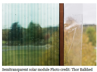
Organic solar cells, made from carbon-based materials, present unique advantages compared with other solar cell technologies. For example, they can be manufactured through low-cost printing technologies, and they can be made semi-transparent with selectable colours, which can be used architecturally in building integration. Their flexibility and low weight make them perfect for powering the sensors for the internet of things applications.
A key challenge facing the development of organic solar cells is that they usually have large energy losses.
Minimise energy losses
“We have formulated some rational design rules to minimise energy losses in organic solar cells. Following these rules, we present a range of examples with low energy losses and high power conversion efficencies”, says Feng Gao, associate professor at the Division of Biomolecular and Organic Electronics at Linköping University.
The design rules, which challenge some previously held ideas, have been published in an article in the prestigious journal Nature Materials.
Using these design rules, organic solar cells promise to catch up with their competitors with respect to power conversion efficiency, which measures the fraction of the energy in the sun’s radiation that is converted to electricity. The theoretical limit for the fraction of the sun’s energy that can be obtained in solar cells is around 33%. Laboratory experiments with silicon-based solar cells have achieved 25% at best. Researchers have until now believed that the limit for organic solar cells is lower.
Semitransparent solar moduleSemitransparent solar module Photo credit: Thor Balkhed“But we now know that there is no difference – the theoretical limit is the same for solar cells manufactured from silicon, perovskites or polymers”, says Olle Inganäs, professor of biomolecular and organic electronics, Linköping university.
Acceptor material is added
When photons from the sun are absorbed by the semiconducting polymer in a solar cell, electrons in the donor material are raised to an excited state, and holes are formed in the ground state to which the electrons remain attracted. In order to separate these bound electrons and holes, an acceptor material is added. However, this acceptor material usually results in extra energy losses, an issue that has bothered the organic solar cell community for over two decades.
What the researchers have now shown is that if the potential difference between donor and acceptor materials is minimised, the electrons only need to make a small transition, and the energy loss can be decreased. The hole that the electrons leave behind even so starts the transport of charge.
However, the minimised potential difference between the donor and acceptor materials does not guarantee low energy losses. Another factor is the heat emitted by certain charge carriers instead of light, which is what is required in an efficient solar cell.
The researchers have also found a solution to the second problem. In order to produce a solar cell that can use as large a fraction of the sun’s spectrum as possible, mixtures of two organic semiconductors are used. One of them has a large bandgap, and the other has a small bandgap. The materials have different high levels of photoluminescence, where the high value means that the electrons most often emit light. In a material with low photoluminescence, heat is produced instead.
“The second rule we have formulated is that the materials with low bandgap have high photoluminescence”, says Feng Gao.
Two fundamental rules
The article in Nature Materials presents two fundamental rules to minimise energy losses for highly efficient organic solar cells:
- Minimise the potential difference between donor and acceptor components.
- Make sure that the low-gap component in the blend has a high photoluminescence.
The researchers at the seven research institutes in the US, China and Europe have together produced around a dozen different materials, some of which have been reported previously and others are completely new. They have used these to demonstrate that the new theory agrees with experimental results, even though it is somewhat incompatible with what was previously believed.
In addition to Feng Gao, Artem A Bakulin from Imperial College London and Veaceslav Coropceanu from the Georgia Institute of Technology are also corresponding authors of the article. The research has been financed by grants from sources in Sweden, the EU, the US and China, and has also been carried out within the framework of the strategic initiative in advanced functional materials, AFM, at Linköping University.
Share on:


Testimonial
"Our marketing partnership with I-Connect007 is already delivering. Just a day after our press release went live, we received a direct inquiry about our updated products!"
Rachael Temple - AlltematedSuggested Items
ITW EAE Despatch Ovens Now Support ASTM 5423 Testing
10/15/2025 | ITW EAEAs the demand for high-performance electrical insulation materials continues to grow—driven by the rapid expansion of electric vehicles (EVs) and energy storage systems—thermal processing has become a critical step in material development.
Beyond Thermal Conductivity: Exploring Polymer-based TIM Strategies for High-power-density Electronics
10/13/2025 | Padmanabha Shakthivelu and Nico Bruijnis, MacDermid Alpha Electronics SolutionsAs power density and thermal loads continue to increase, effective thermal management becomes increasingly important. Rapid and efficient heat transfer from power semiconductor chip packages is essential for achieving optimal performance and ensuring long-term reliability of temperature-sensitive components. This is particularly crucial in power systems that support advanced applications such as green energy generation, electric vehicles, aerospace, and defense, along with high-speed computing for data centers and artificial intelligence (AI).
Is Glass Finally Coming of Age?
10/13/2025 | Nolan Johnson, I-Connect007Substrates, by definition, form the base of all electronic devices. Whether discussing silicon wafers for semiconductors, glass-and-epoxy materials in printed circuits, or the base of choice for interposers, all these materials function as substrates. While other substrates have come and gone, silicon and FR-4 have remained the de facto standards for the industry.
Creative Materials to Showcase Innovative Functional Inks for Medical Devices at COMPAMED 2025
10/09/2025 | Creative Materials, Inc.Creative Materials, a leading manufacturer of high-performance functional inks and coatings, is pleased to announce its participation in COMPAMED 2025, taking place November 17–20 in Düsseldorf, Germany.
Jiva Leading the Charge Toward Sustainable Innovation
09/30/2025 | Marcy LaRont, PCB007 MagazineEnvironmental sustainability in business—product circularity—is a high priority these days. “Circularity,” the term meant to replace “recycling,” in its simplest definition, describes a full circle life for electronic products and all their elements. The result is re-use or a near-complete reintroduction of the base materials back into the supply chain, leaving very little left for waste. For what cannot be reused productively, the ultimate hope is to have better, less harmful means of disposal and/or materials that can seamlessly and harmlessly decompose and integrate back into the natural environment. That is where Jiva and Soluboard come in.