


 American Made Advocacy: Smart Policies Can Ensure AI Data Centers Are Secure
 Beyond the Board: Early Engagement Means Faster Prototyping for Defense Programs
 Defense Speak Interpreted: The Autonomous Plane Battle—Skyborg Vs. Loyal Wingman


Materials Processing Tricks Enable Engineers to Create New Laser Material
July 18, 2018 | UC San DiegoEstimated reading time: 3 minutes
By doping alumina crystals with neodymium ions, engineers at the University of California San Diego have developed a new laser material that is capable of emitting ultra-short, high-power pulses—a combination that could potentially yield smaller, more powerful lasers with superior thermal shock resistance, broad tunability and high-duty cycles.
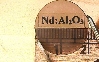
Image caption: Neodymium-alumina laser gain material. Image courtesy of Elias Penilla
To achieve this advance, engineers devised new materials processing strategies to dissolve high concentrations of neodymium ions into alumina crystals. The result, a neodymium-alumina laser gain medium, is the first in the field of laser materials research. It has 24 times higher thermal shock resistance than one of the leading solid-state laser gain materials.
Neodymium and alumina are two of the most widely used components in today’s state-of-the-art solid-state laser materials. Neodymium ions, a type of light-emitting atoms, are used to make high-power lasers. Alumina crystals, a type of host material for light-emitting ions, can yield lasers with ultra-short pulses. Alumina crystals also have the advantage of high thermal shock resistance, meaning they can withstand rapid changes in temperature and high loads of heat.
However, combining neodyumium and alumina to make a lasing medium is challenging. The problem is that they are incompatible in size. Alumina crystals typically host small ions like titanium or chromium. Neodymium ions are too big—they are normally hosted inside a crystal called yttrium aluminum garnet (YAG).
“Until now, it has been impossible to dope sufficient amounts of neodymium into an alumina matrix. We figured out a way to create a neodymium-alumina laser material that combines the best of both worlds: high power density, ultra-short pulses and superior thermal shock resistance,” said Javier Garay, a mechanical engineering professor at the UC San Diego Jacobs School of Engineering.
Cramming More Neodymium Into Alumina
The key to making the neodymium-alumina hybrid was by rapidly heating and cooling the two solids together. Traditionally, researchers dope alumina by melting it with another material and then cooling the mixture slowly so that it crystallizes. “However, this process is too slow to work with neodymium ions as the dopant—they would essentially get kicked out of the alumina host as it crystallizes,” explained first author Elias Penilla, a postdoctoral researcher in Garay’s research group. So his solution was to speed up the heating and cooling steps fast enough to prevent neodymium ions from escaping.
The new process involves rapidly heating a pressurized mixture of alumina and neodymium powders at a rate of 300 C per minute until it reaches 1,260 C. This is hot enough to “dissolve” a high concentration of neodymium into the alumina lattice. The solid solution is held at that temperature for five minutes and then rapidly cooled, also at a rate of 300 C per minute.
Researchers characterized the atomic structure of the neodymium-alumina crystals using X-ray diffraction and electron microscopy. To demonstrate lasing capability, researchers optically pumped the crystals with infrared light (806 nm). The material emitted amplified light (gain) at a lower frequency infrared light at 1064 nm.
Neodymium-alumina (left) shows no signs of cracking at 40 Watts applied voltage, while neodymium-YAG (right) cracks at 25 Watts. Image courtesy of Elias Penilla
In tests, researchers also showed that neodymium-alumina has 24 times higher thermal shock resistance than one of the leading solid-state laser gain materials, neodymium-YAG. “This means we can pump this material with more energy before it cracks, which is why we can use it to make a more powerful laser,” said Garay.
The team is working on building a laser with their new material. “That will take more engineering work. Our experiments show that the material will work as a laser and the fundamental physics is all there,” said Garay.
Paper title: “Gain in Polycrystalline Nd-doped Alumina: Leveraging Length Scales to Create a New Class of High-Energy, Short Pulse, Tunable Laser Materials.” Co-authors include Luis F. Devia-Cruz, Matthew A. Duarte, Corey L. Hardin and Yasuhiro Kodera, all at UC San Diego.
Penilla will be presenting this work as an Invited Oral Lecture on Aug. 19 at the 2018 SPIE Optical Engineering + Application Meeting within the Photonic Fiber and Crystal Devices: Advances in Materials and Innovations in Device Applications XII Section.
This work was supported by the High Energy Laser – Joint Technology Office administered by the Army Research Office.
Share on:


Testimonial
"We’re proud to call I-Connect007 a trusted partner. Their innovative approach and industry insight made our podcast collaboration a success by connecting us with the right audience and delivering real results."
Julia McCaffrey - NCAB GroupSuggested Items
Sealed for Survival: Potting Electronics for the Toughest Environments
10/29/2025 | Beth Massey, MacDermid Alpha Electronics SolutionsElectronics deployed in harsh conditions face relentless threats from vibration, impact, chemical contaminants, airborne pollutants, and moisture, conditions that can quickly lead to failure without robust protection. Potting, the process of encapsulating electronics in a protective polymer, is a widely used strategy to safeguard devices from both environmental and mechanical hazards.
Driving Innovation: Mechanical and Optical Processes During Rigid-flex Production
10/28/2025 | Kurt Palmer -- Column: Driving InnovationRigid-flex printed circuit boards are a highly effective solution for placing complex circuitry in tight, three-dimensional spaces. They are now indispensable across a range of industries, from medical devices and aerospace to advanced consumer electronics, helping designers make the most efficient use of available space. However, their unique construction—combining rigid and flexible materials—presents a fundamental challenge for PCB manufacturers.
SMTAI 2025 Review: Reflecting on a Pragmatic and Forward-looking Industry
10/27/2025 | Marcy LaRont, I-Connect007Leaving the show floor on the final afternoon of SMTA International last week in Rosemont, Illinois, it was clear that the show remains a grounded, technically driven event that delivers a solid program, good networking, and an easy space to commune with industry colleagues and meet with customers.
ITW EAE Despatch Ovens Now Support ASTM 5423 Testing
10/15/2025 | ITW EAEAs the demand for high-performance electrical insulation materials continues to grow—driven by the rapid expansion of electric vehicles (EVs) and energy storage systems—thermal processing has become a critical step in material development.
Beyond Thermal Conductivity: Exploring Polymer-based TIM Strategies for High-power-density Electronics
10/13/2025 | Padmanabha Shakthivelu and Nico Bruijnis, MacDermid Alpha Electronics SolutionsAs power density and thermal loads continue to increase, effective thermal management becomes increasingly important. Rapid and efficient heat transfer from power semiconductor chip packages is essential for achieving optimal performance and ensuring long-term reliability of temperature-sensitive components. This is particularly crucial in power systems that support advanced applications such as green energy generation, electric vehicles, aerospace, and defense, along with high-speed computing for data centers and artificial intelligence (AI).