


 American Made Advocacy: Smart Policies Can Ensure AI Data Centers Are Secure
 Beyond the Board: Early Engagement Means Faster Prototyping for Defense Programs
 Defense Speak Interpreted: The Autonomous Plane Battle—Skyborg Vs. Loyal Wingman


Scientists Reduced the Weight of Optics for Satellite Observation of the Earth by 100 Times
August 9, 2018 | Samara UniversityEstimated reading time: 2 minutes
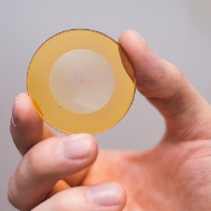
The technology of manufacturing of a 256-layer diffraction harmonic lens and the algorithms for reconstructing the obtained images are described. This optical element, created by the research group of the Department of Supercomputers and General Informatics of Samara University, weighs only 5 grams and replaces a complex and massive system of lenses and mirrors similar to the one that is used in telephoto lenses with a focal length of 300 mm and a weight of 500 grams. "To solve the problems in the areas where there is a constant struggle for the reduction of the weight and size of the optics, such massive systems are not suitable. First of all, it concerns compact systems of Earth remote sensing set on small-sized aircrafts, i.e. UAVs, atmospheric probes and nanosatellites. Ultralight diffraction-optical systems weighing only a few grams open up new possibilities for them", – says one of the authors of the scientific article, Professor of the Department of Supercomputers and General Informatics Artem Nikonorov.
Share on:


Testimonial
"Our marketing partnership with I-Connect007 is already delivering. Just a day after our press release went live, we received a direct inquiry about our updated products!"
Rachael Temple - AlltematedSuggested Items
Cephia Secures $4M Seed Funding to Revolutionize Multimodal Sensing with Metasurface Technology
10/31/2025 | PRNewswireCephia, a startup building products using advanced AI computational imaging technologies and silicon sensors made from advanced metamaterials, formally launched with several pilot customers and $4 million in seed venture capital funding.
KYZEN Honored with 2025 Step-by-Step Excellence Award for Its Innovative ANALYST² Process Control System
10/31/2025 | KYZEN'KYZEN, the global leader in innovative environmentally responsible cleaning chemistries, is proud to announce that its ANALYST² Process Control System has won a 2025 Step-by-Step Excellence Award (SbSEA).
LPKF Delivers Key Strategic Technology to Fraunhofer's Glass Panel Technology Group
10/29/2025 | LPKFLPKF Laser & Electronics SE is one of the initiators of the Glass Panel Technology Group (GPTG), a consortium encompassing the entire process chain for advanced semiconductor packaging with glass substrates.
On the Line With… Ultra HDI Podcast—Episode 7: “Solder Mask: Beyond the Traces,” Now Available
10/31/2025 | I-Connect007I-Connect007 is excited to announce the release of the seventh episode of its 12-part podcast series, On the Line With… American Standard Circuits: Ultra HDI. In this episode, “Solder Mask: Beyond the Traces,” host Nolan Johnson sits down with John Johnson, Director of Quality and Advanced Technology at American Standard Circuits, to explore the essential role that solder mask plays in the Ultra HDI (UHDI) manufacturing process.
Nvidia’s Blackwell Chips Made in Arizona Still Head to Taiwan for Final Assembly
10/27/2025 | I-Connect007 Editorial TeamNvidia has begun production of its next-generation Blackwell GPUs in the United States, but the company still depends heavily on Taiwan to complete the process, The Register reported.