


 SMT Perspectives & Prospects: The Architecture of Winston Churchill’s Leadership
 Global Sourcing Spotlight: Making Global Sourcing Simple Again
 The Government Circuit: New Council Now Helps Shape Policy Decisions in the Electronics Supply Chain


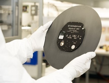
CyberOptics Corporation will demonstrate its next generation airborne particle sensor technology (APS3) 300mm with new ParticleSpectrum software at SEMICON Taiwan, September 5-7 at the Nangang Exhibition Center in Taipei in booth #L312.
CyberOptics’ WaferSense APS3 speeds equipment set-up and long-term yields in semiconductor fabs by wirelessly detecting, identifying and monitoring airborne particles. Now in a thinner and lighter form factor to travel through semiconductor tools with ease, the APS3 offers leading accuracy and sensitivity valued by equipment and process engineers.
“Semiconductor fabs worldwide have adopted our Airborne Particle Sensors,” said Dr. Subodh Kulkarni, president and CEO, CyberOptics. “We have further advanced the technology that they rely on to significantly improve their yields and tool uptime.”
The APS3 solution incorporates ParticleSpectrum software – a completely new, touch-enabled interface with user-friendly functionality, making it simple to read, record and review small to large airborne particle data and see the effects of cleanings, adjustments and repairs in real-time.
At SEMICON Taiwan, CyberOptics will also demonstrate the proprietary 3D ultra high-resolution multi-reflection suppression (MRS) sensor technology that meticulously identifies and rejects reflections caused by shiny components and surfaces. Effective suppression of multiple reflections is critical for highly accurate measurements. Offering an unmatched combination of accuracy and speed, MRS sensors are widely used for inspection and measurement in the SMT, metrology and in semiconductor markets. This best in class, ultra-high-resolution technology used in back-end inspection applications, is ideally suited for IC package, wafer bump inspection and mid-end semiconductor applications where the highest degree of precision is required.
About CyberOptics
CyberOptics Corporation is a leading global developer and manufacturer of high precision sensing technology solutions. CyberOptics’ sensors are used in SMT, semiconductor and metrology markets to significantly improve yields and productivity. By leveraging its leading-edge technologies, the company has strategically established itself as a global leader in high precision 3D sensors, allowing CyberOptics to further increase its penetration of key vertical markets. Headquartered in Minneapolis, Minnesota, CyberOptics conducts worldwide operations through its facilities in North America, Asia and Europe.
For more information about the entire line of CyberOptics solutions please click here.


