


 Driving Innovation: Mechanical and Optical Processes During Rigid-flex Production
 It’s Only Common Sense: Your Biggest Competitor Is Complacency
 The Chemical Connection: Onshoring PCB Production—Daunting but Certainly Possible


Improving Nuclear Detection with New Chip Power
August 22, 2018 | Washington University in St. LouisEstimated reading time: 4 minutes
A cross-disciplinary team of chemists and physicists from Washington University in St. Louis is building a better computer chip to improve detection and surveillance for the illegal transport of nuclear materials at U.S. borders. The work is part of a new, five-year, $10 million collaboration in low-energy nuclear science led by Texas A&M University.
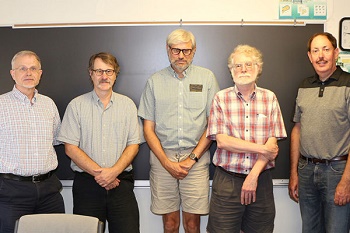
Image Caption: Senior members of the Washington University nuclear program span the chemistry, physics and engineering disciplines, including (from left) Willem Dickhoff, Lee Sobotka, Robert Charity and Jon Elson, along with George Engel (right) of Southern Illinois University Edwardsville (Image: Gary Broyles, Washington University)
Washington University is one of several institutions participating in the Department of Energy/National Nuclear Security Administration’s (DOE/NNSA) Center for Excellence in Nuclear Training and University-based Research (CENTAUR).
Under the new program, Robert J. Charity, research professor of chemistry, and Lee G. Sobotka, professor of chemistry and of physics, both in Arts & Sciences, are testing a novel neutron detection strategy and a related chip. The chip is being developed with long-time collaborator George Engel, a professor in the department of electrical and computer engineering at Southern Illinois University Edwardsville. A kickoff meeting for the CENTAUR collaboration was held Aug. 17.
Roughly two dozen scientists across all partner universities will be involved in CENTAUR, along with their affiliated research groups. One of the center’s major contributions will be research and development expertise related to neutron detectors, which are relevant for both basic low-energy nuclear science and nuclear security applications.
“The problem with existing neutron detectors is that they are too big to get fine position information,” Sobotka said. “They needed to be big to get the required detection efficiency. The solution is to have many — tens of thousands — of small detectors. This had not been contemplated before as it requires a signal processing stream for each of the small detectors.”
A Need for Custom Processing
ASICs — Application-Specific Integrated Circuits — form the backbone for data processing in computers, cell phones and other electronic devices. These custom chips are made because collecting oft-repeated tasks on one chip makes the overall task faster and less expensive to replicate.
Scientists don’t typically get involved with building their own ASICs, unless there is a highly specific need for the custom processing.
ASIC
Electronic design of an Application-Specific Integrated Circuit (ASIC) developed by scientists at Washington University and SIUE. The collaboration has developed chips specifically for studying the properties of, and reactions between, atomic nuclei. (Image: Nuclear & Radiochemistry group)
For example, ASICs are developed for certain high-energy physics experiments, like those done at the European laboratory near Geneva — CERN — where the Higgs boson was discovered. ASICs are also used in some experiments in space and for medical physics devices like the Positron Emission Tomography (PET) device, which was developed by scientists from Washington University 40 years ago.
For their part, Sobotka, Charity and Jon Elson, research engineer in chemistry, teamed up with Engel to build their own ASICs starting in 2001.
The collaboration has recently upgraded two chips that they built and is making a third one honed for a different scientific task. Using the previous versions of just one of these chip designs, the Washington University group has published 25 papers, mostly on the structure of nuclei with exotic neutron-to-proton ratios.
CENTAUR researchers will use two of these chips in tandem, coupled with a particular organic crystal as their detector medium, to complete high-resolution experiments with neutrons that current detectors and signal processing electronics do not allow.
“The NNSA will be closely watching this project,” Sobotka said.
Educating the Next Generation of Science Leaders
CENTAUR is equally committed to building upon the consortium’s collective tradition of service as a technical resource and fertile training ground for the nation’s nuclear workforce and future stewardship science leaders.
In this vein, the Washington University nuclear groups have a long history of technology development, a bug picked up by their students.
Sobotka highlights the technical contributions of an earlier generation of students, including Edward Hoffman and Michael E. Phelps (former students of Demetrios Sarantites, professor of chemistry) for their role in the invention of PET and, more recently, James Dempsey (Sobotka’s former student), who invented the ViewRay technology, which allows for real-time clear imaging of tumors as treatment is being delivered.
“Research that advances basic science, like the work supported by CENTAUR, can inspire students to pursue a career of technical innovation that makes a difference in the lives of people across the country — and around the world,” Sobotka said.
Predicting the location of Neutrons
The CENTAUR grant will also allow the researchers to improve an advanced model that unifies the quantum structure and reactions of nuclei.
Willem H. Dickhoff, professor of physics in Arts & Sciences, who has worked with Charity for a decade, developed this model to predict the location of neutrons in heavy nuclei.
Nuclear scientists have known the proton distribution for decades, but learning the location of neutrons is a far more difficult task.
Knowing where the neutrons are in large nuclei provides insight into the size of neutron stars. Working with physics graduate students Hossein Mahzoon and Mackenzie Atkinson, Dickhoff and Charity recently published work that indicates that — in one nucleus with more neutrons than protons, Ca-48 — more of the excess neutrons are located further from the center than previously thought.
The CENTAUR grant will allow the researchers to expand the model to other nuclei by gathering more data of the type that Charity, Sobotka and their students including Rebecca Shane, Cole Pruitt and undergraduate Jonathan Mueller have collected over the past decade. Interestingly, some of this work can be completed using the synchrocyclotron at the S. Lee Kling Proton Therapy Center at the Siteman Cancer Center.
Share on:


Testimonial
"Our marketing partnership with I-Connect007 is already delivering. Just a day after our press release went live, we received a direct inquiry about our updated products!"
Rachael Temple - AlltematedSuggested Items
Smart Eye Collaborates with Sony on Next-Generation Interior Sensing and Iris Authentication
10/09/2025 | Smart EyeSmart Eye AB, the global leader in Interior Sensing AI and Driver Monitoring Systems (DMS), announced a collaboration with Sony Semiconductor Solutions Corporation (Sony) to integrate Smart Eye’s interior sensing and biometric authentication software with Sony’s newly released IMX775 RGB-IR image sensor.
SEMICON Europa 2025 to Highlight Innovations in Advanced Packaging, Fab Management, and MEMS and Imaging Sensors to Bolster Europe’s Semiconductor Resilience
10/03/2025 | SEMISemiconductor industry experts will convene at SEMICON Europa 2025, November 18-21 at Messe München in Munich, to explore the latest trends and innovations in advanced packaging and fab management.
MEMS & Imaging Sensors Summit to Spotlight Sensing Revolution for Europe’s Leadership
09/11/2025 | SEMIIndustry experts will gather November 19-20 at the SEMI MEMS & Imaging Sensors Summit 2025 to explore the latest breakthroughs in AI-driven MEMS and imaging optimization, AR/VR technologies, and advanced sensor solutions for critical defence applications.
Direct Imaging System Market Size to Hit $4.30B by 2032, Driven by Increasing Demand for High-Precision PCB Manufacturing
09/11/2025 | Globe NewswireAccording to the SNS Insider, “The Direct Imaging System Market size was valued at $2.21 Billion in 2024 and is projected to reach $4.30 Billion by 2032, growing at a CAGR of 8.68% during 2025-2032.”
I-Connect007’s Editor’s Choice: Five Must-Reads for the Week
07/04/2025 | Marcy LaRont, I-Connect007For our industry, we have seen several bullish market announcements over the past few weeks, including one this week by IDC on the massive growth in the global server market. We’re also closely watching global trade and nearshoring. One good example of successful nearshoring is Rehm Thermal Systems, which celebrates its 10th anniversary in Mexico and the official opening of its new building in Guadalajara.