


 Driving Innovation: Mechanical and Optical Processes During Rigid-flex Production
 It’s Only Common Sense: Your Biggest Competitor Is Complacency
 The Chemical Connection: Onshoring PCB Production—Daunting but Certainly Possible


Quantum Simulation Reveals Mobility Edge in a Low-Dimensional Disordered Landscape
August 23, 2018 | University of IllinoisEstimated reading time: 3 minutes
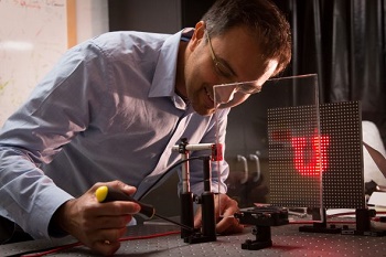
A recent flood of research scholarship on electronic transport in low-dimensional (2D or 1D) materials like graphene or carbon nanotubes reflects the tremendous potential of these materials to unveil a deeper understanding of the laws that govern the sometimes surprising emergent behavior of electrons. Scientists have probed novel materials like these to uncover the physics of topological superconductivity and topological insulators. But one of the biggest challenges researchers face in studying real materials is the presence of uncontrolled impurities that influence electronic transport.
One way to get around this dirty issue of disorder is to study the same types of physical phenomena in artificial materials that have no natural imperfections. In recent decades, researchers have used neutral atoms moving in pristine crystals formed by laser light to perform quantum simulations to observe physical effects that would be hard to see in real electronic materials.
Now scientists at the University of Illinois at Urbana-Champaign using an innovative quantum simulation technique have made one of the first observations of a mobility edge in a low-dimensional system. Physics professor Bryce Gadway and graduate student Fangzhao Alex An were able to combine a disordered virtual material—in this case a pair of coupled 1D chains—with artificial magnetic fields to explore this phenomenon.
An explains, “The artificial magnetic field we engineered causes the neutral atoms in our experiment to behave like electrons in extremely large magnetic fields, equivalent to applying hundreds of Tesla-level magnets. We were able to vary the strength of our artificial magnetic field to tune the properties of our atoms and strongly modify the observed mobility edge.”
So what exactly is a mobility edge? It’s an energy-dependent insulator-to-conductor transition that occurs in disordered systems—a regime of metallic transport that arises out of a special kind of insulator, called an Anderson insulator. Only two groups have ever observed a mobility edge in 3D, and the first was U of I physics professor Brian DeMarco’s research group in 2011. Importantly, the phenomenon is induced by disorder, and according to the laws of localization physics, a mobility edge, let alone any kind of metallic behavior, should not occur in 2D or 1D materials.
Gadway comments, “This observation is truly noteworthy—this kind of behavior shouldn’t occur in lower dimensional systems with random disorder. There’s a subtlety to realizing it in one or two dimensions that relies on a sort of pseudo-random disorder. There are correlations in the disorder we engineered. It turns out this can allow for a metal-insulator transition.”
Gadway continues, “The type of correlated disorder that we used has some very funny properties. In particular, there is a subtle mathematical argument showing that the metal-insulator transition it allows for is completely independent of energy. It turns out that you have to do a little something extra to allow for a mobility edge to arise. In our case, the extra ingredient was creating the large magnetic fields.”
In this research, the scientists also showed evidence for an even more intriguing kind of mobility edge that occurred in the absence of the artificial magnetic fields. This second type of mobility edge came about due to atom-atom interactions, which caused the higher-energy states to behave more strongly like a metal and the lower-energy states to behave more strongly like an insulator.
These results, published August 18, 2018, in Physical Review X, open up new directions in research.
“Going forward,” Gadway concludes, “the next extension of this work will be to explore the interplay of disorder and large magnetic fields in truly two-dimensional systems, not just two coupled chains. This will build on work we’ve been doing on disordered topological insulators in 1D, extending it to the case of disordered quantum Hall systems in 2D.”
Share on:


Testimonial
"The I-Connect007 team is outstanding—kind, responsive, and a true marketing partner. Their design team created fresh, eye-catching ads, and their editorial support polished our content to let our brand shine. Thank you all! "
Sweeney Ng - CEE PCBSuggested Items
Sealed for Survival: Potting Electronics for the Toughest Environments
10/29/2025 | Beth Massey, MacDermid Alpha Electronics SolutionsElectronics deployed in harsh conditions face relentless threats from vibration, impact, chemical contaminants, airborne pollutants, and moisture, conditions that can quickly lead to failure without robust protection. Potting, the process of encapsulating electronics in a protective polymer, is a widely used strategy to safeguard devices from both environmental and mechanical hazards.
Driving Innovation: Mechanical and Optical Processes During Rigid-flex Production
10/28/2025 | Kurt Palmer -- Column: Driving InnovationRigid-flex printed circuit boards are a highly effective solution for placing complex circuitry in tight, three-dimensional spaces. They are now indispensable across a range of industries, from medical devices and aerospace to advanced consumer electronics, helping designers make the most efficient use of available space. However, their unique construction—combining rigid and flexible materials—presents a fundamental challenge for PCB manufacturers.
SMTAI 2025 Review: Reflecting on a Pragmatic and Forward-looking Industry
10/27/2025 | Marcy LaRont, I-Connect007Leaving the show floor on the final afternoon of SMTA International last week in Rosemont, Illinois, it was clear that the show remains a grounded, technically driven event that delivers a solid program, good networking, and an easy space to commune with industry colleagues and meet with customers.
ITW EAE Despatch Ovens Now Support ASTM 5423 Testing
10/15/2025 | ITW EAEAs the demand for high-performance electrical insulation materials continues to grow—driven by the rapid expansion of electric vehicles (EVs) and energy storage systems—thermal processing has become a critical step in material development.
Beyond Thermal Conductivity: Exploring Polymer-based TIM Strategies for High-power-density Electronics
10/13/2025 | Padmanabha Shakthivelu and Nico Bruijnis, MacDermid Alpha Electronics SolutionsAs power density and thermal loads continue to increase, effective thermal management becomes increasingly important. Rapid and efficient heat transfer from power semiconductor chip packages is essential for achieving optimal performance and ensuring long-term reliability of temperature-sensitive components. This is particularly crucial in power systems that support advanced applications such as green energy generation, electric vehicles, aerospace, and defense, along with high-speed computing for data centers and artificial intelligence (AI).