


 Driving Innovation: Mechanical and Optical Processes During Rigid-flex Production
 It’s Only Common Sense: Your Biggest Competitor Is Complacency
 The Chemical Connection: Onshoring PCB Production—Daunting but Certainly Possible


Dual-Layer Solar Cell Developed at UCLA Sets Record for Efficiently Generating Power
August 31, 2018 | UCLAEstimated reading time: 2 minutes
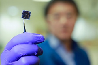
Materials scientists from the UCLA Samueli School of Engineering have developed a highly efficient thin-film solar cell that generates more energy from sunlight than typical solar panels, thanks to its double-layer design.
The device is made by spraying a thin layer of perovskite — an inexpensive compound of lead and iodine that has been shown to be very efficient at capturing energy from sunlight — onto a commercially available solar cell. The solar cell that forms the bottom layer of the device is made of a compound of copper, indium, gallium and selenide, or CIGS.
The team’s new cell converts 22.4% of the incoming energy from the sun, a record in power conversion efficiency for a perovskite–CIGS tandem solar cell. The performance was confirmed in independent tests at the U.S. Department of Energy’s National Renewable Energy Laboratory. (The previous record, set in 2015 by a group at IBM’s Thomas J. Watson Research Center, was 10.9%.) The UCLA device’s efficiency rate is similar to that of the poly-silicon solar cells that currently dominate the photovoltaics market.
“With our tandem solar cell design, we’re drawing energy from two distinct parts of the solar spectrum over the same device area,” Yang said. “This increases the amount of energy generated from sunlight compared to the CIGS layer alone.”
Yang added that the technique of spraying on a layer of perovskite could be easily and inexpensively incorporated into existing solar-cell manufacturing processes.
The cell’s CIGS base layer, which is about 2 microns (or two-thousandths of a millimeter) thick, absorbs sunlight and generates energy at a rate of 18.7% efficiency on its own, but adding the 1 micron-thick perovskite layer improves its efficiency — much like how adding a turbocharger to a car engine can improve its performance. The two layers are joined by a nanoscale interface that the UCLA researchers designed; the interface helps give the device higher voltage, which increases the amount of power it can export.
And the entire assembly sits on a glass substrate that’s about 2 millimeters thick.
“Our technology boosted the existing CIGS solar cell performance by nearly 20% from its original performance,” Yang said. “That means a 20% reduction in energy costs."
He added that devices using the two-layer design could eventually approach 30% power conversion efficiency. That will be the research group’s next goal.
The study’s lead authors are Qifeng Han, a visiting research associate in Yang’s laboratory, and Yao-Tsung Hsieh and Lei Meng, who both recently earned their doctorates at UCLA. The study’s other authors are members of Yang’s research group and researchers from Solar Frontier Corp.’s Atsugi Research Center in Japan.
The research was supported by the National Science Foundation and the Air Force Office of Scientific Research. Yang and his research group have been working on tandem solar cells for several years and their accomplishments include developing transparent tandem solar cells that could be used in windows.
Share on:


Testimonial
"We’re proud to call I-Connect007 a trusted partner. Their innovative approach and industry insight made our podcast collaboration a success by connecting us with the right audience and delivering real results."
Julia McCaffrey - NCAB GroupSuggested Items
WestDev Announces Advanced Thermal Analysis Integration for Pulsonix PCB Design Suite
10/29/2025 | WestDev Ltd.Pulsonix, the industry-leading PCB design software from WestDev Ltd., announced a major enhancement to its design ecosystem: a direct interface between Pulsonix and ADAM Research's TRM (Thermal Risk Management) analysis software.
Designers Notebook: Power and Ground Distribution Basics
10/29/2025 | Vern Solberg -- Column: Designer's NotebookThe principal objectives to be established during the planning stage are to define the interrelationship between all component elements and confirm that there is sufficient surface area for placement, the space needed to ensure efficient circuit interconnect, and to accommodate adequate power and ground distribution.
Episode 6 of Ultra HDI Podcast Series Explores Copper-filled Microvias in Advanced PCB Design and Fabrication
10/15/2025 | I-Connect007I-Connect007 has released Episode 6 of its acclaimed On the Line with... American Standard Circuits: Ultra High Density Interconnect (UHDI) podcast series. In this episode, “Copper Filling of Vias,” host Nolan Johnson once again welcomes John Johnson, Director of Quality and Advanced Technology at American Standard Circuits, for a deep dive into the pros and cons of copper plating microvias—from both the fabricator’s and designer’s perspectives.
Nolan’s Notes: Tariffs, Technologies, and Optimization
10/01/2025 | Nolan Johnson -- Column: Nolan's NotesLast month, SMT007 Magazine spotlighted India, and boy, did we pick a good time to do so. Tariff and trade news involving India was breaking like a storm surge. The U.S. tariffs shifted India from one of the most favorable trade agreements to the least favorable. Electronics continue to be exempt for the time being, but lest you think that we’re free and clear because we manufacture electronics, steel and aluminum are specifically called out at the 50% tariff levels.
MacDermid Alpha & Graphic PLC Lead UK’s First Horizontal Electroless Copper Installation
09/30/2025 | MacDermid Alpha & Graphic PLCMacDermid Alpha Electronics Solutions, a leading supplier of integrated materials and chemistries to the electronics industry, is proud to support Graphic PLC, a Somacis company, with the installation of the first horizontal electroless copper metallization process in the UK.