


 Driving Innovation: Mechanical and Optical Processes During Rigid-flex Production
 It’s Only Common Sense: Your Biggest Competitor Is Complacency
 The Chemical Connection: Onshoring PCB Production—Daunting but Certainly Possible


Watching Two-Dimensional Materials Grow
August 31, 2018 | TU WienEstimated reading time: 2 minutes
They are among the thinnest structures on earth: “two dimensional materials” are crystals which consist of only one or a few layers of atoms. They often display unusual properties, promising many new applications in opto-electronics and energy technology. One of these materials is 2D-molybdenum sulphide, an atomically thin layer of molybdenum and sulphur atoms.
The production of such ultra-thin crystals is difficult. The crystallisation process depends on many different factors. In the past, different techniques have yielded quite diverse results, but the reasons for this could not be accurately explained. Thanks to a new method developed by research teams at TU Wien, the University of Vienna and Joanneum Research in Styria, for the first time ever it is now possible to observe the crystallisation process directly under the electron microscope. The method has now been presented in the scientific journal ‘ACS nano’.
From Gas to Crystal
“Molybdenum sulphide can be used in transparent and flexible solar cells or for sustainably generating hydrogen for energy storage”, says the lead author of the study, Bernhard C. Bayer from the Institute of Materials Chemistry at TU Wien. “In order to do this, however, high-quality crystals must be grown under controlled conditions.”
Usually this is done by starting out with atoms in gaseous form and then condensing them on a surface in a random and unstructured way. In a second step, the atoms are arranged in regular crystal form – through heating, for example. “The diverse chemical reactions during the crystallisation process are, however, still unclear, which makes it very difficult to develop better production methods for 2D materials of this kind”, Bayer states.
Thanks to a new method, however, it should now be possible to accurately study the details of the crystallisation process. “This means it is no longer necessary to experiment through trial and error, but thanks to a deeper understanding of the processes, we can say for certain how to obtain the desired product”, Bayer adds.
Graphene as a Substrate
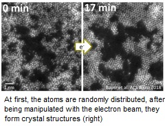
First, molybdenum and sulphur are placed randomly on a membrane made of graphene. Graphene is probably the best known of the 2D materials – a crystal with a thickness of only one atom layer consisting of carbon atoms arranged in a honeycomb lattice. The randomly arranged molybdenum and sulphur atoms are then manipulated in the electron microscope with a fine electron beam. The same electron beam can be used simultaneously to image the process and to initiate the crystallization process.
That way it has now become possible for the first time to directly observe how the atoms move and rearrange during the growth of the material with a thickness of only two atomic layers. “In doing so, we can see that the most thermodynamically stable configuration doesn't necessarily always have to be the final state”, Bayer says. Different crystal arrangements compete with one another, transform into each other and replace one another. “Therefore, it is now clear why earlier investigations had such varying results. We are dealing with a complex, dynamic process.” The new findings will help to adapt the structure of the 2D materials more precisely to application requirements in future by interfering with the rearrangement processes in a targeted manner.
Share on:


Testimonial
"In a year when every marketing dollar mattered, I chose to keep I-Connect007 in our 2025 plan. Their commitment to high-quality, insightful content aligns with Koh Young’s values and helps readers navigate a changing industry. "
Brent Fischthal - Koh YoungSuggested Items
Sealed for Survival: Potting Electronics for the Toughest Environments
10/29/2025 | Beth Massey, MacDermid Alpha Electronics SolutionsElectronics deployed in harsh conditions face relentless threats from vibration, impact, chemical contaminants, airborne pollutants, and moisture, conditions that can quickly lead to failure without robust protection. Potting, the process of encapsulating electronics in a protective polymer, is a widely used strategy to safeguard devices from both environmental and mechanical hazards.
Driving Innovation: Mechanical and Optical Processes During Rigid-flex Production
10/28/2025 | Kurt Palmer -- Column: Driving InnovationRigid-flex printed circuit boards are a highly effective solution for placing complex circuitry in tight, three-dimensional spaces. They are now indispensable across a range of industries, from medical devices and aerospace to advanced consumer electronics, helping designers make the most efficient use of available space. However, their unique construction—combining rigid and flexible materials—presents a fundamental challenge for PCB manufacturers.
SMTAI 2025 Review: Reflecting on a Pragmatic and Forward-looking Industry
10/27/2025 | Marcy LaRont, I-Connect007Leaving the show floor on the final afternoon of SMTA International last week in Rosemont, Illinois, it was clear that the show remains a grounded, technically driven event that delivers a solid program, good networking, and an easy space to commune with industry colleagues and meet with customers.
ITW EAE Despatch Ovens Now Support ASTM 5423 Testing
10/15/2025 | ITW EAEAs the demand for high-performance electrical insulation materials continues to grow—driven by the rapid expansion of electric vehicles (EVs) and energy storage systems—thermal processing has become a critical step in material development.
Beyond Thermal Conductivity: Exploring Polymer-based TIM Strategies for High-power-density Electronics
10/13/2025 | Padmanabha Shakthivelu and Nico Bruijnis, MacDermid Alpha Electronics SolutionsAs power density and thermal loads continue to increase, effective thermal management becomes increasingly important. Rapid and efficient heat transfer from power semiconductor chip packages is essential for achieving optimal performance and ensuring long-term reliability of temperature-sensitive components. This is particularly crucial in power systems that support advanced applications such as green energy generation, electric vehicles, aerospace, and defense, along with high-speed computing for data centers and artificial intelligence (AI).