


 Driving Innovation: Mechanical and Optical Processes During Rigid-flex Production
 It’s Only Common Sense: Your Biggest Competitor Is Complacency
 The Chemical Connection: Onshoring PCB Production—Daunting but Certainly Possible


Diamond Dust Enables Low-Cost, High-Efficiency Magnetic Field Detection
September 12, 2018 | UC BerkeleyEstimated reading time: 3 minutes
UC Berkeley engineers have created a device that dramatically reduces the energy needed to power magnetic field detectors, which could revolutionize how we measure the magnetic fields that flow through our electronics, our planet and even our bodies.
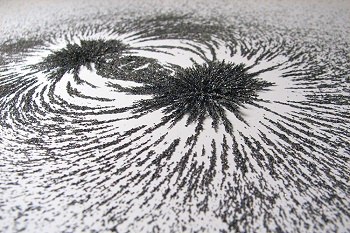
Image Caption: A new device developed by UC Berkeley engineers provides low-cost, high-efficiency magnetic field detection. (Credit: Windell Oskay, via Flickr)
“The best magnetic sensors out there today are bulky, only operate at extreme temperatures and can cost tens of thousands of dollars,” said Dominic Labanowski, who helped create the device, which is made from nitrogen-infused diamonds, as a postdoctoral researcher in the Department of Electrical Engineering and Computer Science. “Our sensors could replace those more-difficult-to-use sensors in a lot of applications from navigation to medical imaging to natural resource exploration.”
Each time a diamond-based sensor measures a magnetic field, it must first be blasted with 1 to 10 watts of microwave radiation to prime them to be sensitive to magnetic fields, which is enough power to melt electronic components. The researchers found a new way to excite tiny diamonds with microwaves using 1,000 times less power, making it feasible to create magnetic-sensing devices that can fit into electronics like cell phones.
This work was led by the lab of EECS professor Sayeef Salahuddin at UC Berkeley in collaboration with researchers from the Ohio State University. The team reports their device online Sep. 7 in the journal Science Advances.
Defective Diamonds
Bombarding a diamond with a jet of nitrogen gas can knock out some of its highly ordered carbon atoms, replacing them with nitrogen atoms. These nitrogen interlopers — called nitrogen vacancy (NV) centers — have unique properties that are well understood by scientists.
“You can use these NV centers as very powerful sensors, but traditionally their applications have been limited because it takes a lot of power to read them,” said Labanowski.
A Greenish Yellow Colored Film with Black Spots
In the device, which is about the size of a fingernail, clusters of diamond nanocrystals (black spots) sit atop a material called a multiferroic. The multiferroic transmits microwave energy into the crystals much more efficiently than other methods.
To detect magnetic fields, scientists first have to hit the NV centers with high-powered microwave radiation, equal to about one-hundredth the power of your standard microwave or 10 times the power consumed by an average cell phone. They then illuminate the NV centers with a laser, which is absorbed and emitted by the nitrogen atoms.
Image Caption: The strength of the magnetic field is related to the strength of the emitted laser light: the intensity of the emitted light can be used to measure the field strength.
To create the device, the researchers placed diamond nanocrystals — containing thousands of NV centers apiece — onto a film called a multiferroic. This new type of material is capable of transferring microwave energy to the crystals much more efficiently.
“This technique dramatically lowers the power consumption of the sensors and makes them usable for realistic applications,” Labanowski said.
Imaging Inside the Body and Under the Earth
Medical applications of magnetic sensors include magnetoencephalography, which uses magnetic fields to measure brain waves, or magnetocardiography, which uses magnetic fields to image heart function. Currently these machines are the size of a small room and can cost upwards of $3 million.
“With low-power NV sensors, you could imagine taking a room-sized magnetoencephalography machine and turning it into something like a helmet, dramatically reducing the size and the costs,” Labanowski said.
The sensors could also be placed in planes or drones to aid in spotting rare earth metals underground, or used in cell phones to improve navigation.
Magnetic field detection is just one application of NV centers, Salahuddin says. The team is planning to refine their technology to use NV centers and other types of quantum systems in a wide variety of applications.
“While we emphasized magnetic field sensing, our work could lead to electrical manipulation of quantum systems in general with much broader areas of application including quantum computing,” Salahuddin said.
Co-authors of the paper are V. Praveen Bhallamudi, Qiaochi Guo, Carola M. Purser and Brendan A. McCullian from the Department of Physics at The Ohio State University.
Share on:


Testimonial
"We’re proud to call I-Connect007 a trusted partner. Their innovative approach and industry insight made our podcast collaboration a success by connecting us with the right audience and delivering real results."
Julia McCaffrey - NCAB GroupSuggested Items
Smart Eye Collaborates with Sony on Next-Generation Interior Sensing and Iris Authentication
10/09/2025 | Smart EyeSmart Eye AB, the global leader in Interior Sensing AI and Driver Monitoring Systems (DMS), announced a collaboration with Sony Semiconductor Solutions Corporation (Sony) to integrate Smart Eye’s interior sensing and biometric authentication software with Sony’s newly released IMX775 RGB-IR image sensor.
SEMICON Europa 2025 to Highlight Innovations in Advanced Packaging, Fab Management, and MEMS and Imaging Sensors to Bolster Europe’s Semiconductor Resilience
10/03/2025 | SEMISemiconductor industry experts will convene at SEMICON Europa 2025, November 18-21 at Messe München in Munich, to explore the latest trends and innovations in advanced packaging and fab management.
MEMS & Imaging Sensors Summit to Spotlight Sensing Revolution for Europe’s Leadership
09/11/2025 | SEMIIndustry experts will gather November 19-20 at the SEMI MEMS & Imaging Sensors Summit 2025 to explore the latest breakthroughs in AI-driven MEMS and imaging optimization, AR/VR technologies, and advanced sensor solutions for critical defence applications.
Direct Imaging System Market Size to Hit $4.30B by 2032, Driven by Increasing Demand for High-Precision PCB Manufacturing
09/11/2025 | Globe NewswireAccording to the SNS Insider, “The Direct Imaging System Market size was valued at $2.21 Billion in 2024 and is projected to reach $4.30 Billion by 2032, growing at a CAGR of 8.68% during 2025-2032.”
I-Connect007’s Editor’s Choice: Five Must-Reads for the Week
07/04/2025 | Marcy LaRont, I-Connect007For our industry, we have seen several bullish market announcements over the past few weeks, including one this week by IDC on the massive growth in the global server market. We’re also closely watching global trade and nearshoring. One good example of successful nearshoring is Rehm Thermal Systems, which celebrates its 10th anniversary in Mexico and the official opening of its new building in Guadalajara.