


 Driving Innovation: Mechanical and Optical Processes During Rigid-flex Production
 It’s Only Common Sense: Your Biggest Competitor Is Complacency
 The Chemical Connection: Onshoring PCB Production—Daunting but Certainly Possible


Nano-Sandwiching Improves Heat Transfer, Prevents Overheating in Nanoelectronics
September 13, 2018 | UICEstimated reading time: 2 minutes
Sandwiching two-dimensional materials used in nanoelectronic devices between their three-dimensional silicon bases and an ultrathin layer of aluminum oxide can significantly reduce the risk of component failure due to overheating, according to a new study published in the journal of Advanced Materials led by researchers at the University of Illinois at Chicago College of Engineering.
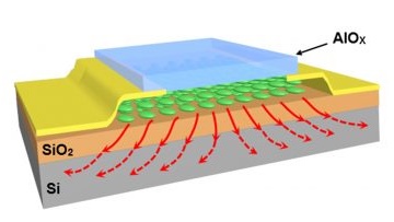
Image Caption: An experimental transistor using silicon oxide for the base, carbide for the 2D material and aluminum oxide for the encapsulating material (Image: Zahra Hemmat).
Many of today’s silicon-based electronic components contain 2D materials such as graphene. Incorporating 2D materials like graphene — which is composed of a single-atom-thick layer of carbon atoms — into these components allows them to be several orders of magnitude smaller than if they were made with conventional, 3D materials. In addition, 2D materials also enable other unique functionalities. But nanoelectronic components with 2D materials have an Achilles’ heel — they are prone to overheating. This is because of poor heat conductance from 2D materials to the silicon base.
“In the field of nanoelectronics, the poor heat dissipation of 2D materials has been a bottleneck to fully realizing their potential in enabling the manufacture of ever-smaller electronics while maintaining functionality,” said Amin Salehi-Khojin, associate professor of mechanical and industrial engineering in UIC’s College of Engineering.
One of the reasons 2D materials can’t efficiently transfer heat to silicon is that the interactions between the 2D materials and silicon in components like transistors are rather weak.
“Bonds between the 2D materials and the silicon substrate are not very strong, so when heat builds up in the 2D material, it creates hot spots causing overheat and device failure,” explained Zahra Hemmat, a graduate student in the UIC College of Engineering and co-first author of the paper.
In order to enhance the connection between the 2D material and the silicon base to improve heat conductance away from the 2D material into the silicon, engineers have experimented with adding an additional ultra-thin layer of material on top of the 2D layer — in effect creating a “nano-sandwich” with the silicon base and ultrathin material as the “bread.”
“By adding another ‘encapsulating’ layer on top of the 2D material, we have been able to double the energy transfer between the 2D material and the silicon base,” Salehi-Khojin said.
Salehi-Khojin and his colleagues created an experimental transistor using silicon oxide for the base, carbide for the 2D material and aluminum oxide for the encapsulating material. At room temperature, the researchers saw that the conductance of heat from the carbide to the silicon base was twice as high with the addition of the aluminum oxide layer versus without it.
“While our transistor is an experimental model, it proves that by adding an additional, encapsulating layer to these 2D nanoelectronics, we can significantly increase heat transfer to the silicon base, which will go a long way towards preserving functionality of these components by reducing the likelihood that they burn out,” said Salehi-Khojin. “Our next steps will include testing out different encapsulating layers to see if we can further improve heat transfer.”
Poya Yasaei, Zahra Hemmat, Liang Hong, Amirhossein Behranginia, Leily Majidi and Robert Klie from the University of Illinois at Chicago; Cameron Foss and Zlatan Aksamija, from the University of Massachusetts, Amherst, and Shixuan Li and Michel Barsoum from Drexel University are co-authors on the paper.
This research was supported in part by grants EFRI 2-DARE Grant 1542864, DMR-0959470 and DMR-1626065 from the National Science Foundation.
Share on:


Testimonial
"Your magazines are a great platform for people to exchange knowledge. Thank you for the work that you do."
Simon Khesin - Schmoll MaschinenSuggested Items
Sealed for Survival: Potting Electronics for the Toughest Environments
10/29/2025 | Beth Massey, MacDermid Alpha Electronics SolutionsElectronics deployed in harsh conditions face relentless threats from vibration, impact, chemical contaminants, airborne pollutants, and moisture, conditions that can quickly lead to failure without robust protection. Potting, the process of encapsulating electronics in a protective polymer, is a widely used strategy to safeguard devices from both environmental and mechanical hazards.
Driving Innovation: Mechanical and Optical Processes During Rigid-flex Production
10/28/2025 | Kurt Palmer -- Column: Driving InnovationRigid-flex printed circuit boards are a highly effective solution for placing complex circuitry in tight, three-dimensional spaces. They are now indispensable across a range of industries, from medical devices and aerospace to advanced consumer electronics, helping designers make the most efficient use of available space. However, their unique construction—combining rigid and flexible materials—presents a fundamental challenge for PCB manufacturers.
SMTAI 2025 Review: Reflecting on a Pragmatic and Forward-looking Industry
10/27/2025 | Marcy LaRont, I-Connect007Leaving the show floor on the final afternoon of SMTA International last week in Rosemont, Illinois, it was clear that the show remains a grounded, technically driven event that delivers a solid program, good networking, and an easy space to commune with industry colleagues and meet with customers.
ITW EAE Despatch Ovens Now Support ASTM 5423 Testing
10/15/2025 | ITW EAEAs the demand for high-performance electrical insulation materials continues to grow—driven by the rapid expansion of electric vehicles (EVs) and energy storage systems—thermal processing has become a critical step in material development.
Beyond Thermal Conductivity: Exploring Polymer-based TIM Strategies for High-power-density Electronics
10/13/2025 | Padmanabha Shakthivelu and Nico Bruijnis, MacDermid Alpha Electronics SolutionsAs power density and thermal loads continue to increase, effective thermal management becomes increasingly important. Rapid and efficient heat transfer from power semiconductor chip packages is essential for achieving optimal performance and ensuring long-term reliability of temperature-sensitive components. This is particularly crucial in power systems that support advanced applications such as green energy generation, electric vehicles, aerospace, and defense, along with high-speed computing for data centers and artificial intelligence (AI).