


 Driving Innovation: Mechanical and Optical Processes During Rigid-flex Production
 It’s Only Common Sense: Your Biggest Competitor Is Complacency
 The Chemical Connection: Onshoring PCB Production—Daunting but Certainly Possible


Shrinking Semiconductor Lasers to the Nanoscale
September 14, 2018 | A*STAREstimated reading time: 2 minutes
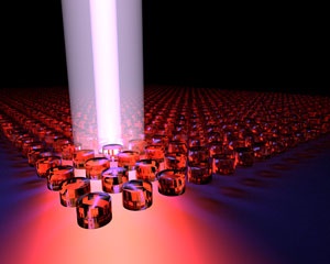
A tiny laser comprising an array of nanoscale semiconductor cylinders (see image) has been made by an all-A*STAR team. This is the first time that lasing has been achieved in non-metallic nanostructures, and it promises to lead to miniature lasers usable in a wide range of optoelectronic devices.
Microscale lasers are widely used in devices such as CD and DVD players. Now, optical engineers are developing nanoscale lasers — so small that they cannot be seen by the human eye.
A promising method is to use arrays of tiny structures made from semiconductors with a high refractive index. Such structures act as tiny antennas, resonating at specific wavelengths. However, it has been challenging to use them to construct a cavity — the heart of a laser, where light bounces around while being amplified.
Now, Arseniy Kuznetsov, Son Tung Ha, Ramón Paniagua-Domínguez, and their colleagues at the A*STAR Institute of Materials Research and Engineering have overcome this problem by exploiting a highly unusual type of standing wave that remains in one spot despite coexisting with a continuous spectrum of radiating waves that can transport energy away. First predicted by quantum mechanics, this wave was demonstrated experimentally in optics about a decade ago.
There was an element of serendipity in the invention. “We initially planned to create a laser just based on the diffractive resonances in the array,” recalls Kuznetsov. “But after fabricating samples and testing them, we discovered this strong enhancement at a different wavelength from expected. When we went back and did further simulations and analysis, we realized that we had created these special waves.”
The demonstration is the culmination of five years of research by the team. It was a race against time, since other groups were also working on developing active nanoantennas, Kuznetsov notes. “Until now, lasing hasn’t been realized in nanoantenna structures,” he says. “So it’s a big step for the dielectric nanoantenna community.”
Their laser also has advantages over other kinds of miniature lasers. Firstly, the direction of its narrow, well-defined beam can be easily controlled — this maneuverability is often needed in device applications. Also, because the nanocylinders are quite sparsely distributed, the laser is highly transparent, which is beneficial for multilayer devices that contain other optical components.
The team is now working to develop lasers that can be excited electrically, rather than by light as in the present study, which would be a major advance toward realizing commercial nanolasers.
Share on:


Testimonial
"In a year when every marketing dollar mattered, I chose to keep I-Connect007 in our 2025 plan. Their commitment to high-quality, insightful content aligns with Koh Young’s values and helps readers navigate a changing industry. "
Brent Fischthal - Koh YoungSuggested Items
Electra’s ElectraJet EMJ110 Inkjet Soldermask Now in Black & Blue at Sunrise Electronics
09/08/2025 | Electra Polymers LtdFollowing the successful deployment of Electra’s Green EMJ110 Inkjet Soldermask on KLA’s Orbotech Neos™ platform at Sunrise Electronics in Elk Grove Village, Illinois, production has now moved beyond green.
Magnachip Semiconductor Announces YJ Kim to Step Down as CEO; Current Board Chairman Camillo Martino Appointed Interim CEO
08/14/2025 | PR NewswireMagnachip Semiconductor Corporation today announced that YJ Kim has agreed to step down as CEO and as a member of the Board of Directors, effective immediately. Camillo Martino, Chairman of the Board of Directors, has also been appointed Interim Chief Executive Officer, effective immediately.
Bell to Build X-Plane for Phase 2 of DARPA Speed and Runway Independent Technologies (SPRINT) X-Plane Program
07/09/2025 | Bell Textron Inc.Bell Textron Inc., a Textron Inc. company, has been down-selected for Phase 2 of Defense Advanced Research Projects Agency (DARPA) Speed and Runway Independent Technologies (SPRINT) X-Plane program with the objective to complete design, construction, ground testing and certification of an X-plane demonstrator.
Nolan’s Notes: Moving Forward With Confidence
06/03/2025 | Nolan Johnson -- Column: Nolan's NotesWe’re currently enjoying a revitalized and dynamic EMS provider market with significant growth potential. Since December 2024, the book-to-bill has been extremely strong and growing. Starting with a ratio of 1.24 in December, book-to-bill has continued to accelerate to a 1.41 in April. Yet, there is a global economic restructuring taking place. To say that the back-and-forth with tariffs and trade deals makes for an uncertain market is an understatement. While we may be in a 90-day tariff pause among leading economic nations, the deadline is quickly approaching and that leaves many of you feeling unsettled about what to expect.
Mycronic High Flex Changes Division Name to PCB Assembly Solutions
05/20/2025 | MycronicMycronic AB, the leading Sweden-based electronics assembly solutions provider, announced that its division formerly known as High Flex will now operate under the name PCB Assembly Solutions.