


 Driving Innovation: Mechanical and Optical Processes During Rigid-flex Production
 It’s Only Common Sense: Your Biggest Competitor Is Complacency
 The Chemical Connection: Onshoring PCB Production—Daunting but Certainly Possible


Multibit Optoelectronic Memory
September 21, 2018 | NUSEstimated reading time: 2 minutes
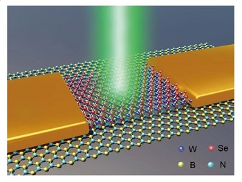
NUS scientists have developed multibit optoelectronic memory using a heterostructure made of two-dimensional (2D) materials for next generation devices.
Optoelectronic memories are devices which can store photon-generated charge carriers when exposed to light. The stored charges can be accessed later for information retrieval. These devices can be used in image capture and spectrum analysis systems. 2D atomically layered materials are promising candidates for the development of next generation optoelectronic memories to meet emerging requirements for device miniaturisation and structural flexibility. However, optoelectronic memories fabricated using 2D materials have been reported to suffer from poor data storage capability with the highest reported figure at about eight distinct storage states.
A team lead by Prof CHEN Wei from both the Department of Chemistry and the Department of Physics, NUS has developed a multibit, non-volatile optoelectronic memory device that is able to store up to 130 distinct states by using a tungsten diselenide/ boron nitride (WSe2/ BN) heterostructure. The heterostructure, made of 2D materials, comprises a monolayer of WSe2 on a 20-layer BN. The programming (store data) and erasing (delete data) functions are controlled by adjusting the applied polarity to the device. A negative polarity is applied during the programming function and it causes the photon-generated electrons from the midgap donor-like states of the BN material to transfer into the WSe2 material. This leaves behind localised (non-mobile) positive charges in the BN material. For the erasing function, a positive polarity is applied. This causes the photon-generated electrons from the valence band in the BN material to recombine with the localised positive charges, returning it to a neutral state.
The amount of electrons transferred into the WSe2 material is dependent on the duration of light exposure time for the device. A longer exposure time would mean that more electrons are transferred. The researchers found that the continual accumulation of electrons in the WSe2 material corresponding up to 130 light pulses can be detected before saturation conditions set in. Each of these pulses can be treated as a distinct storage state. During performance testing, they found that the device exhibits a data retention of over 4.5×10⁴ seconds and a cyclic programme/ erase endurance exceeding 200 cycles.
Explaining the significance of the findings, Prof Chen said, “Although there is still a performance gap when compared to commercial silicon-based memory, these devices are advantageous in electronic applications which require structural flexibility. The use of this WSe2/ BN 2D layered heterostructure provides a method to achieve multibit memory device and may pave the way for the development of next generation optoelectronic memories.”
Share on:


Testimonial
"Our marketing partnership with I-Connect007 is already delivering. Just a day after our press release went live, we received a direct inquiry about our updated products!"
Rachael Temple - AlltematedSuggested Items
Sealed for Survival: Potting Electronics for the Toughest Environments
10/29/2025 | Beth Massey, MacDermid Alpha Electronics SolutionsElectronics deployed in harsh conditions face relentless threats from vibration, impact, chemical contaminants, airborne pollutants, and moisture, conditions that can quickly lead to failure without robust protection. Potting, the process of encapsulating electronics in a protective polymer, is a widely used strategy to safeguard devices from both environmental and mechanical hazards.
Driving Innovation: Mechanical and Optical Processes During Rigid-flex Production
10/28/2025 | Kurt Palmer -- Column: Driving InnovationRigid-flex printed circuit boards are a highly effective solution for placing complex circuitry in tight, three-dimensional spaces. They are now indispensable across a range of industries, from medical devices and aerospace to advanced consumer electronics, helping designers make the most efficient use of available space. However, their unique construction—combining rigid and flexible materials—presents a fundamental challenge for PCB manufacturers.
SMTAI 2025 Review: Reflecting on a Pragmatic and Forward-looking Industry
10/27/2025 | Marcy LaRont, I-Connect007Leaving the show floor on the final afternoon of SMTA International last week in Rosemont, Illinois, it was clear that the show remains a grounded, technically driven event that delivers a solid program, good networking, and an easy space to commune with industry colleagues and meet with customers.
ITW EAE Despatch Ovens Now Support ASTM 5423 Testing
10/15/2025 | ITW EAEAs the demand for high-performance electrical insulation materials continues to grow—driven by the rapid expansion of electric vehicles (EVs) and energy storage systems—thermal processing has become a critical step in material development.
Beyond Thermal Conductivity: Exploring Polymer-based TIM Strategies for High-power-density Electronics
10/13/2025 | Padmanabha Shakthivelu and Nico Bruijnis, MacDermid Alpha Electronics SolutionsAs power density and thermal loads continue to increase, effective thermal management becomes increasingly important. Rapid and efficient heat transfer from power semiconductor chip packages is essential for achieving optimal performance and ensuring long-term reliability of temperature-sensitive components. This is particularly crucial in power systems that support advanced applications such as green energy generation, electric vehicles, aerospace, and defense, along with high-speed computing for data centers and artificial intelligence (AI).