


 Driving Innovation: Mechanical and Optical Processes During Rigid-flex Production
 It’s Only Common Sense: Your Biggest Competitor Is Complacency
 The Chemical Connection: Onshoring PCB Production—Daunting but Certainly Possible


Researchers Create Smartphone System to Test for Lead in Water
September 27, 2018 | University of HoustonEstimated reading time: 2 minutes
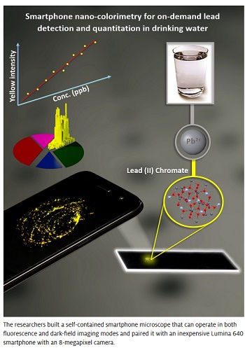
The discovery of lead in Flint, Michigan’s drinking water drew renewed attention to the health risks posed by the metal. Now researchers at the University of Houston have created an inexpensive system using a smartphone and a lens made with an inkjet printer that can detect lead in tap water at levels commonly accepted as dangerous.
The system builds upon earlier work by Wei-Chuan Shih, associate professor of electrical & computer engineering, and members of his lab, including the discovery of an inexpensive elastomer lens that can convert a basic smartphone into a microscope.
The latest discovery, described in the journal Analytical Chemistry, combines nano-colorimetry with dark-field microscopy, integrated into the smartphone microscope platform to detect levels of lead below the safety threshold set by the Environmental Protection Agency.
“Smartphone nano-colorimetry is rapid, low-cost, and has the potential to enable individual citizens to examine (lead) content in drinking water on-demand in virtually any environmental setting,” the researchers wrote.
Even small amounts of lead can cause serious health problems, with young children especially vulnerable to neurological damage. EPA standards require lead levels in drinking water to be below 15 parts per billion, and Shih said currently available consumer test kits aren’t sensitive enough to accurately detect lead at that level.
By using an inexpensive smartphone equipped with an inkjet-printed lens and using the dark-field imaging mode, researchers were able to produce a system that was both portable and easy to operate, as well as able to detect lead concentrations at 5 parts per billion in tap water. The sensitivity reached 1.37 parts per billion in deionized water.
Shih and his students last year published an open-source dataset in Biomedical Optics Express, explaining how to convert a smartphone equipped with the elastomer lens into a microscope capable of fluorescence microscopy. That paper has been the journal’s most frequently downloaded paper since its publication.
The latest application incorporates color analysis to detect nanoscale lead particles. In addition to Shih, researchers on the project include first author Hoang Nguyen and Yulung Sung, Kelly O’Shaughnessy and Xiaonan Shan, all with the UH Department of Electrical & Computer Engineering. (O’Shaughnessy was a summer intern from the University of Cincinnati under the National Science Foundation’s Research Experiences for Undergraduates program.)
Applying the dataset published in 2017, the researchers built a self-contained smartphone microscope that can operate in both fluorescence and dark-field imaging modes and paired it with an inexpensive Lumina 640 smartphone with an 8-megapixel camera. They spiked tap water with varying amounts of lead, ranging from 1.37 parts per billion to 175 parts per billion. They then added chromate ions, which react with the lead to form lead chromate nanoparticles; the nanoparticles can be detected by combining colorimetric analysis and microscopy.
The analysis measured both the intensity detected from the nanoparticles, correlating that to the lead concentration, and verified that the reaction was spurred by the presence of lead.
The mixture was transferred to a polydimethylsiloxane slab attached to a glass slide; after it dried, deionized water was used to rinse off the chromate compound and the remaining sediment was imaged for analysis.
The microscopy imaging capability proved essential, Shih said, because the quantity of sediment was too small to be imaged with an unassisted smartphone camera, making it impossible to detect relatively low levels of lead.
Building upon the smartphone microscope platform to create a useful consumer product was key, Shih said. “We wanted to be sure we could do something that would be useful from the standpoint of detecting lead at the EPA standard,” he said.
Share on:


Testimonial
"In a year when every marketing dollar mattered, I chose to keep I-Connect007 in our 2025 plan. Their commitment to high-quality, insightful content aligns with Koh Young’s values and helps readers navigate a changing industry. "
Brent Fischthal - Koh YoungSuggested Items
Five Ways to Revolutionize EMS Sales With AI
10/22/2025 | Nolan Johnson, SMT007 MagazineIf you’ve been in the EMS game for any length of time, you know the sales cycle can be a challenge to navigate. It’s complex, technical, and often a marathon, not a sprint. With OEMs demanding faster turnarounds, tighter margins, and bulletproof supply chains, the pressure is on for EMS providers to stand out in a crowded field.
Hardware Engineers, Manufacturing Leaders Ready to ‘Build Better’ Electronics
10/06/2025 | Marcy LaRont, I-Connect007According to Instrumental’s dynamic CEO, Anna-Katrina Shedletsky, the Build Better Electronics Manufacturing Summit on Sept. 30 was a passion project meant to provide a forum for hardware engineering senior leadership, who have very busy jobs and limited opportunities, to share information, thought leadership, and networking opportunities. “Build Better is really about cross-pollination and sharing,” she said, as she highlighted the importance of supporting this type of sharing in tech, which may be more important than ever before.
Dan’s Biz Bookshelf: Four Important Books You Need to Read (Not Just Say You Have)
09/18/2025 | Dan Beaulieu -- Column: Dan's Biz BookshelfDan Beaulieu continues his popular book review series by reviewing four classic books that he believes everyone should have on their bookshelf. In this column, he reviews "The Prince" by Niccolò Machiavelli, "The Art of War," by Sun Tzu, "How to Win Friends and Influence People," by Dale Carnegie, and "Think and Grow Rich," by Napoleon Hill. While we've all heard of these books and maybe read them, Dan will give you a new perspective.
Intel Announces Key Leadership Appointments to Accelerate Innovation and Strengthen Execution
09/09/2025 | Intel CorporationIntel Corporation today announced a series of senior leadership appointments that support the company’s strategy to strengthen its core product business, build a trusted foundry, and foster a culture of engineering across the business.
Summit Interconnect Announces Appointment of Leo LaCroix as Chief Operating Officer
09/09/2025 | Summit Interconnect, Inc.Summit Interconnect, a leading North American manufacturer of Printed Circuit Boards (PCBs), today announced that Leo LaCroix has assumed the role of Chief Operating Officer (COO).