


 Driving Innovation: Mechanical and Optical Processes During Rigid-flex Production
 It’s Only Common Sense: Your Biggest Competitor Is Complacency
 The Chemical Connection: Onshoring PCB Production—Daunting but Certainly Possible


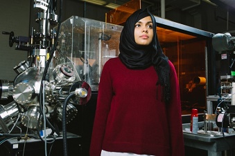
When Takian Fakhrul was a young girl, her father, then a graduate student in materials science at the University of Manchester, would bring her along to his lab. During these visits, she would peek at structures under the microscopes or watch him polish newly synthesized materials. And she just couldn’t seem to stay silent.
“I used to ask a lot of questions,” says Fakhrul, who is now a fourth-year PhD student in MIT's Department of Materials Science and Engineering. “My dad tells me that I was a super-curious child.”
Fakhrul’s curiosity blossomed further when she was an undergraduate at Bangladesh University of Engineering and Technology in her hometown of Dhaka, Bangladesh. Conversations with her father, who was then a materials science professor there, figured heavily into her decision to major in the same field. They talked about pressing scientific problems, like the limits of existing materials and breakthroughs in materials science that could “really affect the future of technology,” Fakhrul recalls.
Now, working in the lab of Caroline Ross, the Toyota Professor of Materials Science and Engineering, Fakhrul researches how garnets can solve problems in photonics, the study of the technical applications of light.
After finishing her PhD, she plans to return to Bangladesh to teach materials science and mentor students who want to pursue graduate studies. She hopes to help advance the field in her home country, drawing from some of the ingenuity she’s observed at MIT and at Indian Institute of Technology Delhi, where her colleagues have found creative ways to conduct their materials science research despite having far fewer resources. “I’ll take back my expertise, the connections I make here, and hopefully I’ll be able to create a bridge between MIT and Bangladesh,” she says.
Breaking Speed Limits
Within computers, data moves between and within chips electronically through small copper wires. In an increasingly technology-dominated world, “computers need to work faster and faster,” Fakhrul says. In order to do that, scientists must design chips and connections that allow faster data transfers and lower power consumption.
“The problem is that there’s a limit to the speed of electrons passing through metal wires,” Fakhrul says. “What’s faster than electrons in metal? The answer to that is light.” And, unlike metal wires, which can carry only a single electronic data stream, optical fibers can carry multiple wavelengths of light — and thus multiple data streams and more bandwidth — without interference. Optical fibers are already being used in networking and storage area networks; the key to advanced optical communication, and maybe even computing with light, is to design fast and energy-efficient optical fiber interconnects that function well on silicon chips.
Fakhrul researches materials for optical isolators — a component of lasers used in silicon photonics that provide a one-way path through which light can travel. “It lets light pass in the forward direction, but not backward. And that’s extremely important,” Fakhrul says. “Back reflections going into the laser destabilize the laser, reducing its performance.”
“If you really want to integrate silicon photonics onto a chip, then you definitely need to have this optical isolator integrated as well,” Fakhrul says.
Fakhrul focuses on iron garnets, which often experience chemical substitution — a trait that gives materials scientists the opportunity to design new variations of the material. The transparent nature of garnet allows light to pass through without interference. Iron garnets are also magnetic, such that they can rotate the plane of polarization of the light as it travels through. “When light passes through garnet, it acts differently in one direction than in the other direction,” Fakhrul says. By manipulating the garnets to design one-way streets for light, she hopes to demonstrate that garnets are the ideal materials for integrated optical isolators. But they also come with a catch.
“[Garnets are] actually very difficult to integrate on silicon,” Fakhrul says. “So that’s something that materials scientists have to deal with and figure out.”
Fakhrul is also interested in how garnets could be used to improve information processing. In an emerging field known as magnonics, information is transferred via the collective precession of spin waves — disturbances that propagate through magnetic materials. In garnets, spin waves “travel for long distances without relaxing,” Fakhrul says, due to their low damping constants.
“You can have this one class of materials, but then it has these unique properties that make it interesting for these versatile applications,” Fakhrul says.
Cherishing Community
After earning her undergraduate degree, Fakhrul was hired as a lecturer at Bangladesh University of Engineering and Technology and began to teach other materials science students while she completed her master’s in materials science.
During her master’s program, she also married her colleague, Nadim Chowdhury, who was a lecturer in electrical engineering and, like Fakhrul, planning to pursue a PhD.
A month into their marriage, Fakhrul recalls, “I got my acceptance letter from MIT, and he got his acceptance letter from Princeton. We were really thinking about long-distance. But a week later, he got into MIT as well! It was so amazing — it was like a miracle,” Fakhrul says.
Together, Fakhrul and her husband moved to Cambridge, and they began their studies at MIT. To stay in touch with her cultural heritage, Fakhrul became involved in the Bangladeshi Students Association at MIT, which hosts events with national, cultural, and religious significance throughout the year. This year, Fakhrul will be a co-president of the student group after working as a secretary for two years and an organization chair for one.
Page 1 of 2
Share on:


Testimonial
"In a year when every marketing dollar mattered, I chose to keep I-Connect007 in our 2025 plan. Their commitment to high-quality, insightful content aligns with Koh Young’s values and helps readers navigate a changing industry. "
Brent Fischthal - Koh YoungSuggested Items
WestDev Announces Advanced Thermal Analysis Integration for Pulsonix PCB Design Suite
10/29/2025 | WestDev Ltd.Pulsonix, the industry-leading PCB design software from WestDev Ltd., announced a major enhancement to its design ecosystem: a direct interface between Pulsonix and ADAM Research's TRM (Thermal Risk Management) analysis software.
Designers Notebook: Power and Ground Distribution Basics
10/29/2025 | Vern Solberg -- Column: Designer's NotebookThe principal objectives to be established during the planning stage are to define the interrelationship between all component elements and confirm that there is sufficient surface area for placement, the space needed to ensure efficient circuit interconnect, and to accommodate adequate power and ground distribution.
Episode 6 of Ultra HDI Podcast Series Explores Copper-filled Microvias in Advanced PCB Design and Fabrication
10/15/2025 | I-Connect007I-Connect007 has released Episode 6 of its acclaimed On the Line with... American Standard Circuits: Ultra High Density Interconnect (UHDI) podcast series. In this episode, “Copper Filling of Vias,” host Nolan Johnson once again welcomes John Johnson, Director of Quality and Advanced Technology at American Standard Circuits, for a deep dive into the pros and cons of copper plating microvias—from both the fabricator’s and designer’s perspectives.
Nolan’s Notes: Tariffs, Technologies, and Optimization
10/01/2025 | Nolan Johnson -- Column: Nolan's NotesLast month, SMT007 Magazine spotlighted India, and boy, did we pick a good time to do so. Tariff and trade news involving India was breaking like a storm surge. The U.S. tariffs shifted India from one of the most favorable trade agreements to the least favorable. Electronics continue to be exempt for the time being, but lest you think that we’re free and clear because we manufacture electronics, steel and aluminum are specifically called out at the 50% tariff levels.
MacDermid Alpha & Graphic PLC Lead UK’s First Horizontal Electroless Copper Installation
09/30/2025 | MacDermid Alpha & Graphic PLCMacDermid Alpha Electronics Solutions, a leading supplier of integrated materials and chemistries to the electronics industry, is proud to support Graphic PLC, a Somacis company, with the installation of the first horizontal electroless copper metallization process in the UK.