


 It’s Only Common Sense: The Phone Is Still Mightier Than the Keyboard
 The Marketing Minute: Marketing With Layers


Efficient Light Conversion with Perovskite Nanocrystals
October 12, 2018 | University of AmsterdamEstimated reading time: 3 minutes
Perovskites are a family of crystals that show promising properties for applications in nano-technology. However, one useful property that until now was unobserved in perovskites is so-called carrier multiplication—an effect that makes materials much more efficient in converting light into electricity. New research, led by UvA-IoP physicists Dr Chris de Weerd and Dr Leyre Gomez from the group of Prof. Tom Gregorkiewicz, has now shown that certain perovskites in fact do have this desirable property.
Crystals are configurations of atoms, molecules or ions, that are ordered in a structure that repeats itself in all directions. We have all encountered some crystals in everyday life: ordinary salt, diamond and even snowflakes are examples. What is perhaps less well-known is that certain crystals show very interesting properties when their size is not that of our everyday life but that of nanometers—a few billionths of a meter. There, we enter the world of nanocrystals, structures that have shown to be extremely useful in constructing technological applications at tiny scales.
Perovskites—named after 19th century Russian mineralogist Lev Perovski—form a particular family of materials that all share the same crystal structure. These perovskites have many desirable electronic properties, making them useful for constructing for example LEDs, TV-screens, solar cells and lasers. For this reason, the perovskites have been studied extensively by physicists in the past years.
Carrier Multiplication
A property which so far had not been shown to exist in perovskites is carrier multiplication. When semiconductors—in solar cells, for example—convert the energy of light into electricity, this is usually done one particle at a time: a single infalling photon results in a single excited electron (and the corresponding ‘hole’ where the electron used to be) that can carry an electrical current. However, in certain materials, if the infalling light is energetic enough, further electron-hole pairs can be excited as a result; it is this process that is known as carrier multiplication.
When carrier multiplication occurs, the conversion from light into electricity can become much more efficient. For example, in ordinary solar cells there is a theoretical limit (the so-called Shockley-Queisser limit) on the amount of energy that can be converted in this way: at most a little over 33% of the solar power gets turned into electrical power. In semiconductor nanocrystals that feature the carrier multiplication effect, however, a maximum efficiency of up to 44% is predicted.
PhD
This makes it very interesting to search for the carrier multiplication effect in perovskites as well, and that is precisely what UvA-IoP physicists Chris de Weerd and Leyre Gomez from the Optoelectronic Materials group led by Prof. Tom Gregorkiewicz, in collaboration with the group of Prof. Yasufumi Fujiwara and with support of their colleagues from the AIST National Institute in Tsukuba and the Delft University of Technology have now done. Using spectroscopy methods—studying the frequencies of the radiation that comes from a material after very briefly illuminating it with a flash of light—the researchers showed that perovskite nanocrystals made out of cesium, lead and iodine, do indeed display carrier multiplication. Moreover, they argue that the efficiency of this effect is higher than reported thus far for any other materials; with this finding therefore, the extraordinary properties of perovskites receive a new boost.
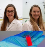
De Weerd, who successfully defended her PhD thesis based on this and other research last week, says: “Until now, carrier multiplication had not been reported for perovskites. That we have now found it is of great fundamental impact on this upcoming material. For example, this shows that perovskite nanocrystals can be used to construct very efficient photodetectors, and in the future perhaps solar cells.”
Share on:


Testimonial
"The I-Connect007 team is outstanding—kind, responsive, and a true marketing partner. Their design team created fresh, eye-catching ads, and their editorial support polished our content to let our brand shine. Thank you all! "
Sweeney Ng - CEE PCBSuggested Items
ITW EAE Despatch Ovens Now Support ASTM 5423 Testing
10/15/2025 | ITW EAEAs the demand for high-performance electrical insulation materials continues to grow—driven by the rapid expansion of electric vehicles (EVs) and energy storage systems—thermal processing has become a critical step in material development.
Beyond Thermal Conductivity: Exploring Polymer-based TIM Strategies for High-power-density Electronics
10/13/2025 | Padmanabha Shakthivelu and Nico Bruijnis, MacDermid Alpha Electronics SolutionsAs power density and thermal loads continue to increase, effective thermal management becomes increasingly important. Rapid and efficient heat transfer from power semiconductor chip packages is essential for achieving optimal performance and ensuring long-term reliability of temperature-sensitive components. This is particularly crucial in power systems that support advanced applications such as green energy generation, electric vehicles, aerospace, and defense, along with high-speed computing for data centers and artificial intelligence (AI).
Is Glass Finally Coming of Age?
10/13/2025 | Nolan Johnson, I-Connect007Substrates, by definition, form the base of all electronic devices. Whether discussing silicon wafers for semiconductors, glass-and-epoxy materials in printed circuits, or the base of choice for interposers, all these materials function as substrates. While other substrates have come and gone, silicon and FR-4 have remained the de facto standards for the industry.
Creative Materials to Showcase Innovative Functional Inks for Medical Devices at COMPAMED 2025
10/09/2025 | Creative Materials, Inc.Creative Materials, a leading manufacturer of high-performance functional inks and coatings, is pleased to announce its participation in COMPAMED 2025, taking place November 17–20 in Düsseldorf, Germany.
Jiva Leading the Charge Toward Sustainable Innovation
09/30/2025 | Marcy LaRont, PCB007 MagazineEnvironmental sustainability in business—product circularity—is a high priority these days. “Circularity,” the term meant to replace “recycling,” in its simplest definition, describes a full circle life for electronic products and all their elements. The result is re-use or a near-complete reintroduction of the base materials back into the supply chain, leaving very little left for waste. For what cannot be reused productively, the ultimate hope is to have better, less harmful means of disposal and/or materials that can seamlessly and harmlessly decompose and integrate back into the natural environment. That is where Jiva and Soluboard come in.