


 It’s Only Common Sense: The Phone Is Still Mightier Than the Keyboard
 The Marketing Minute: Marketing With Layers


Basking in a Quantum Efficiency Glow
October 22, 2018 | KAISTEstimated reading time: 1 minute
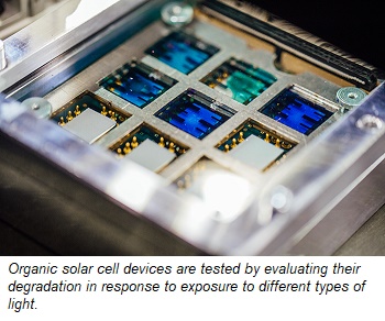
New houses could soon deliver on a long-awaited promise and incorporate windows or roof tiles that harvest solar energy, research conducted at KAUST suggests.
Derya Baran, at the KAUST Solar Center, and her colleagues have developed a photovoltaic organic material that captures light efficiently and that potentially could be coated on building materials.
Traditional roof-mounted solar panels are made from slabs of silicon, but organic molecules can also capture energy from sunlight. These molecules could be formulated as inexpensive printable inks that are applied to regular building components such as windows. Turning sunlight into electricity is a multistep process, and the key to developing high-performance organic photovoltaic materials has been to find organic molecules that are good at every step, Baran explains.
When light strikes an organic photovoltaic material it knocks free an electron, leaving behind a positively charged hole. If the oppositely charged electron and hole recombine, the captured energy is lost. Thus, organic solar cells incorporate a mixture of electron donor and electron acceptor molecules to draw the charges apart.
“When I started my postgraduate studies in 2015, there was a lot of hype about fullerene buckyball derivatives as acceptors, and record efficiencies were around 10-11 percent with poor stabilities,” Baran recalls. But fullerenes have several drawbacks—not least, relatively poor light absorption—so Baran has been investigating nonfullerene acceptors. “Now efficiencies up to 17% are being reported,” she says. “I believe these acceptors will shape the future of organic photovoltaics.”
The nonfullerene acceptor, known as EHIDTBR, assessed by Baran and her colleagues offers several advantages: The team showed that as well as strongly absorbing visible light, it mixed well with the electron donor component, which is important for long-term stability and performance.
EHIDTBR was also very efficient at dissociating excitons and preventing recombination—a property that should make for easy manufacturing, Baran says. In materials where recombination is high, the light-harvesting layer must be very thin so that the charges quickly reach the electrode layer, minimizing their chance to recombine. But these ultrathin layers are challenging to manufacture. “Thicker films are easier to print, particularly when they need to be scaled up for manufacturing,” Baran says.
Scaling up the technology is the team’s next step, Baran adds. “We have a spin-out company from KAUST Solar Center and through this company we want to make photovoltaic windows for electricity generation.”
Share on:


Testimonial
"The I-Connect007 team is outstanding—kind, responsive, and a true marketing partner. Their design team created fresh, eye-catching ads, and their editorial support polished our content to let our brand shine. Thank you all! "
Sweeney Ng - CEE PCBSuggested Items
Samsung Cuts 2nm Wafer Prices to Undercut TSMC
09/30/2025 | I-Connect007 Editorial TeamSamsung Electronics has lowered the price of its 2-nanometer wafers to approximately $20,000, undercutting rival Taiwan Semiconductor Manufacturing Co. (TSMC) by about one-third, Digitimes reported on September 29.
Weaning the U.S. Military Off a Tablet Supply Chain That Leads to China
09/08/2025 | Jim Will, USPAETablet computers are essential to how our military fights, moves and sustains, but these devices are built on a fragile global supply chain with strong ties to China. Building domestic manufacturing to eliminate this vulnerability is feasible if we tap into the information and capabilities that already exist and create strong demand for tablets produced by trusted and assured sources.
Fresh PCB Concepts: Designing for Success at the Rigid-flex Transition Area
08/28/2025 | Team NCAB -- Column: Fresh PCB ConceptsRigid-flex PCBs come in all shapes and sizes. Manufacturers typically use fire-retardant, grade 4 (FR-4) materials in the rigid section and flexible polyimide materials in the flex region. Because of the small size, some rigid-flex PCBs, like those for hearing aid devices, are among the most challenging to manufacture. However, regardless of its size, we should not neglect the transition area between the rigid and flexible material.
Semiconductors Get Magnetic Boost with New Method from UCLA Researchers
07/31/2025 | UCLA NewsroomA new method for combining magnetic elements with semiconductors — which are vital materials for computers and other electronic devices — was unveiled by a research team led by the California NanoSystems Institute at UCLA.
Japan’s OHISAMA Project Aims to Beam Solar Power from Space This Year
07/14/2025 | I-Connect007 Editorial TeamJapan could be on the cusp of making history with its OHISAMA project in its quest to become the first country to transmit solar power from space to Earth, The Volt reported.