


 It’s Only Common Sense: The Phone Is Still Mightier Than the Keyboard
 The Marketing Minute: Marketing With Layers


Materials for the Photonics of Tomorrow
October 24, 2018 | University of BremenEstimated reading time: 3 minutes
Motivated by the success story of the super-thin “miracle material” graphene, which was awarded the Nobel Prize for Physics a few years ago, researchers in chemistry and physics today are continuously discovering new, atomically thin materials. They consist of lattices of atoms that are only slightly thicker than the individual atoms themselves. The pioneer graphene is composed of a single layer of carbon atoms. Although it is excellently suited for electronics, it is not suitable for optical applications. Now there are new atomically thin materials that are suitable for highly miniaturized and extremely energy-efficient optical components. It is remarkable how easy and inexpensive the new materials can be manufactured: they can, for example, be removed with adhesive film from so-called volume crystals.
Wide Range of Applications
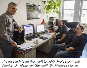
A central idea here is the principle of the “Lego construction kit”: the properties of luminescent and electrically conductive atomically thin materials, such as transition metal dichalcogenides (TMDs), are combined with graphene by stacking them directly on top of each other. Despite loose cohesion, these structures exhibit enormous mechanical stability. The TMDs they contain not only shine very well, but also absorb light and can convert it into electricity. This is why the first practical applications are already available in very sensitive sensors. They can also be used in flexible solar panels or smartphone displays. By using them in highly miniaturized lasers, new components can be realized that are needed for the high-speed Internet of the next generation. “With these materials, we can provide a whole pool of components for innovations in engineering and technology. The properties of these atomically thin flakes are highly interesting in light of the growing demand for renewable and efficient energy sources,” explains Frank Jahnke, Professor of Theoretical Physics. Together with Dr. Matthias Florian and Dr. Alexander Steinhoff, he conducted the investigations at the University of Bremen.
Atomic Physics in Two Dimensions
For physicists, the atomically thin layers also mean a radical rethink. In contrast to conventional atomic physics, which always refers to a three-dimensional space, everything here takes place in only two spatial directions. In order to make the layers glow, the electrons in the atoms must be excited. Positive and negative charges then generate new composite particles or artificial atoms, which can only move in the plane of the thin network. Physicists now have to formulate a two-dimensional atomic physics that presents them with numerous puzzles. In particular, they want to understand the characteristic spectral lines of the particles, which they can measure with spectroscopic methods – similar to the investigation of gas molecules in our atmosphere. “Although these particle complexes in crystals are much more short lived than real atoms and molecules, they can be made visible in modern ultrafast experiments,” explains junior researcher Dr. Alexander Steinhoff.
Research into Spectral Fingerprint of Materials
In close cooperation with colleagues from experimental physics in Berlin and Houston, Texas, the team from the University of Bremen has combined computer simulations with state-of-the-art spectroscopy to obtain the spectral fingerprint of these composite particles. They have shown that the inner structure of the four-particle complexes gives rise to new quantum states. These go far beyond the previously known laws of atomic and molecular physics, because they generate a rich spectral signature.
From Basic Research to Application
The scientists have now published their discoveries in the renowned journal “Nature Physics.” With their findings, they help to bring order to the so-called line zoo of the new materials, because they provide colleagues in their research field with a recipe for identifying further lines. The results are interesting for basic research because they go far beyond the usual analogy between solid-state and atomic physics. The researchers are also keeping a close eye on the applications: as a next step, they plan to produce functional prototypes of such components.
Share on:


Testimonial
"We’re proud to call I-Connect007 a trusted partner. Their innovative approach and industry insight made our podcast collaboration a success by connecting us with the right audience and delivering real results."
Julia McCaffrey - NCAB GroupSuggested Items
ITW EAE Despatch Ovens Now Support ASTM 5423 Testing
10/15/2025 | ITW EAEAs the demand for high-performance electrical insulation materials continues to grow—driven by the rapid expansion of electric vehicles (EVs) and energy storage systems—thermal processing has become a critical step in material development.
Beyond Thermal Conductivity: Exploring Polymer-based TIM Strategies for High-power-density Electronics
10/13/2025 | Padmanabha Shakthivelu and Nico Bruijnis, MacDermid Alpha Electronics SolutionsAs power density and thermal loads continue to increase, effective thermal management becomes increasingly important. Rapid and efficient heat transfer from power semiconductor chip packages is essential for achieving optimal performance and ensuring long-term reliability of temperature-sensitive components. This is particularly crucial in power systems that support advanced applications such as green energy generation, electric vehicles, aerospace, and defense, along with high-speed computing for data centers and artificial intelligence (AI).
Is Glass Finally Coming of Age?
10/13/2025 | Nolan Johnson, I-Connect007Substrates, by definition, form the base of all electronic devices. Whether discussing silicon wafers for semiconductors, glass-and-epoxy materials in printed circuits, or the base of choice for interposers, all these materials function as substrates. While other substrates have come and gone, silicon and FR-4 have remained the de facto standards for the industry.
Creative Materials to Showcase Innovative Functional Inks for Medical Devices at COMPAMED 2025
10/09/2025 | Creative Materials, Inc.Creative Materials, a leading manufacturer of high-performance functional inks and coatings, is pleased to announce its participation in COMPAMED 2025, taking place November 17–20 in Düsseldorf, Germany.
Jiva Leading the Charge Toward Sustainable Innovation
09/30/2025 | Marcy LaRont, PCB007 MagazineEnvironmental sustainability in business—product circularity—is a high priority these days. “Circularity,” the term meant to replace “recycling,” in its simplest definition, describes a full circle life for electronic products and all their elements. The result is re-use or a near-complete reintroduction of the base materials back into the supply chain, leaving very little left for waste. For what cannot be reused productively, the ultimate hope is to have better, less harmful means of disposal and/or materials that can seamlessly and harmlessly decompose and integrate back into the natural environment. That is where Jiva and Soluboard come in.