


 It’s Only Common Sense: The Phone Is Still Mightier Than the Keyboard
 The Marketing Minute: Marketing With Layers


Nanocrystals Arrange to Improve Electronics
October 26, 2018 | Lawrence Livermore National LaboratoryEstimated reading time: 2 minutes
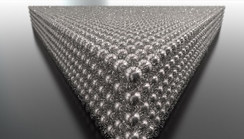
Lawrence Livermore National Laboratory (LLNL) researchers are working to make better electronic devices by delving into the way nanocrystals are arranged inside of them.
Nanocrystals are promising building blocks for new and improved electronic devices, due to their size-tunable properties and ability to integrate into devices at low-cost.
While the structure of nanocrystals has been extensively studied, no one has been able to watch the full assembly process.
That’s where LLNL scientists Christine Orme, Yixuan Yu, Babak Sadigh and a colleague from the University of California, Los Angeles come in.
‘We think the situation can be improved if detailed quantitative information on the nanocrystal assembly process could be identified and if the crystallization process were better controlled,” said Orme, an LLNL material scientist and corresponding author of a paper appearing in the journal Nature Communications.
Nanocrystals inside devices form ensembles, whose collective physical properties, such as charge carrier mobility, depend on both the properties of individual nanocrystals and the way they are arranged. In principle, ordered nanocrystal ensembles, or superlattices, allow for more control in charge transport by facilitating the formation of minibands. However, in practice, few devices built from ordered nanocrystal superlattices are on the market.
Most previous studies use solution evaporation methods to generate nanocrystal superlattices and probe the assembly process as the solvent is being gradually removed. It is difficult to obtain quantitative information on the assembly process, however, because the volume and shape of the nanocrystal solution is continually changing in an uncontrollable manner and the capillary forces can drive nanocrystal motion during drying.
Electric field-driven growth offers a solution to this problem. “We have recently demonstrated that an electric field can be used to drive the assembly of well-ordered, 3D nanocrystal superlattices,” Orme said.
Because the electric field increases the local concentration without changing the volume, shape or composition of nanocrystal solution, the crystallizing system can be probed quantitatively without complications associated with capillary forces or scattering from drying interfaces.
As anticipated, the team found that the electric field drives nanocrystals toward the surface, creating a concentration gradient that leads to nucleation and growth of superlattices. Surprisingly, the field also sorts the particles according to size. In essence, the electric field both concentrates and purifies the nanocrystal solution during growth.
“Because of this size sorting effect, the superlattice crystals are better ordered and the size of the nanocrystals in the lattice can be tuned during growth,” Orme said. “This might be a useful tool for optoelectronic devices. We’re working on infrared detectors now and think it might be an interesting strategy for improving color in monitors.”
Share on:


Testimonial
"Advertising in PCB007 Magazine has been a great way to showcase our bare board testers to the right audience. The I-Connect007 team makes the process smooth and professional. We’re proud to be featured in such a trusted publication."
Klaus Koziol - atgSuggested Items
ITW EAE to Showcase Latest Electronic Assembly Equipment Developments at productronica
10/21/2025 | ITWITW EAE will be showcasing its latest developments at productronica, November 18-21 in Munich, Germany. The ITW EAE booth A4–554 will have MPM, Camalot, Electrovert, Vitronics Soltec and Despatch applications experts on hand as well as sales and management to answer questions and offer solutions.
PCBA Market Poised to Reach $147.5 Billion by 2035
10/20/2025 | Globe NewswireGlobal printed circuit board assembly market is projected to reach $147.5 billion by 2035, at a CAGR of 4.7% during the forecast period 2025-2035
Precision PCB Acquires Assets of Microplace
10/13/2025 | Precision Technologies Inc.Precision Technologies Inc., doing business as Precision PCB, a One-Stop PCB Fabrication and Assembly services company with 27 years of experience providing Quality, Reliability and Excellence in customer service, has acquired the assets of Microplace, Inc.
ZenaTech Advances Taiwan Facility to Commissioning for NDAA-Compliant Drone Component Production
10/08/2025 | Globe NewswireZenaTech, Inc., a business technology solution provider specializing in AI (Artificial Intelligence) drones, Drone as a Service (DaaS), Enterprise SaaS, and Quantum Computing solutions, announces that its Taipei, Taiwan-based Spider Vision Sensors (SVS) subsidiary has advanced to the commissioning phase and assembly line setup at its recently leased 16,000 square-foot drone components manufacturing facility.
Dymax's New 9773 Ruggedized Adhesive Meets NASA ASTM E595 Low Outgassing
10/07/2025 | DymaxDymax, a leading manufacturer of rapid and light-curing materials and equipment, is pleased to add 9773 ruggedizing and staking adhesive to its portfolio of materials designed for coating, protecting, and securing components on printed circuit boards in satellites, missiles, and space applications.