


 It’s Only Common Sense: The Phone Is Still Mightier Than the Keyboard
 The Marketing Minute: Marketing With Layers


Scientists Obtain New Class of Curved Beams for Biosensors and Nanoparticle Control
October 26, 2018 | Tomsk Polytechnic UniversityEstimated reading time: 2 minutes
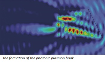
A new class of curved plasmon beams named as a photonic hook plasmon was obtained by researchers from Tomsk Polytechnic University and the Institute of Ultra High-Frequency Semiconductor Electronics of the Russian Academy of Sciences. Due to their small size, they can be used as a nanoparticle manipulator, as well as in biosensors to study substances in small volumes and plasmon microscopes for benefiting superresolution. The findings of the study were published in Annalen der Physik.
A plasmon is a quasi-particle that occurs in solids or near their surface due to electron oscillations. Surface plasmons interact strongly with light; therefore, they determine certain optical properties of metals. Since 2007, scientists have known the only type of curvilinear plasmon waves occurring on the surface of metals, i.e. the Airy rays and their derivatives.
"I should mention that the formation of curvilinear plasmon hooks has so far been possible only on the basis of the Airy family that requires a rather sophisticated and time-consuming method.
We proposed a new class of curved surface plasmon wave, the photonic hook plasmon (PHP), which is fundamentally simpler to generate and has the curvature of beams close to the size of the plasmon wavelength. It is based on the interaction of the surface plasmon wave with a dielectric layer of a special non-symmetric form," says a leader of the project, TPU Professor Igor V. Minin from the Division of Electronic Engineering.
The search of principles to create novel curved beams is an exciting modern field of research that is opening wide fundamental and practical prospects.
In the study, the authors used dielectric particles, e.g. fluoroplastic, with a size of two wavelengths, located on a metal surface. One side of the particle is made in the form of a prism and the second is a square. As the researchers note, particles of different forms can also be used to generate a photonic plasmon hook.
“A flat plasmon wave falls on the conical part of the dielectric, passes through the particle and on the back, square side a focused curvilinear region appears. In shape, it is similar to a hook. Earlier, we successfully used this method for photons and now we demonstrated that the method is appropriate to plasmons too,” clarifies Igor Minin.
The obtained photonic plasmon hook has an important advantage over the Airy rays, i.e. it is much smaller. The curvature of beams is close to the size of the plasmon wavelength, which represents the smallest radius of curvature ever recorded for the SPP beam and makes it possible to use it at the nanoscale.
"In practice such plasmon beams are of interest for biomedical applications, e.g. for biosensors and the synthesis of advanced materials, devices for optical manipulation, e.g. for switching optical signals, and for obtaining new molecules because the ‘hook’ due to its properties can bring together atoms of different elements and much more. This area of research is just in the very beginning of its long journey," says the scientist.
Share on:


Testimonial
"Advertising in PCB007 Magazine has been a great way to showcase our bare board testers to the right audience. The I-Connect007 team makes the process smooth and professional. We’re proud to be featured in such a trusted publication."
Klaus Koziol - atgSuggested Items
Beyond Thermal Conductivity: Exploring Polymer-based TIM Strategies for High-power-density Electronics
10/13/2025 | Padmanabha Shakthivelu and Nico Bruijnis, MacDermid Alpha Electronics SolutionsAs power density and thermal loads continue to increase, effective thermal management becomes increasingly important. Rapid and efficient heat transfer from power semiconductor chip packages is essential for achieving optimal performance and ensuring long-term reliability of temperature-sensitive components. This is particularly crucial in power systems that support advanced applications such as green energy generation, electric vehicles, aerospace, and defense, along with high-speed computing for data centers and artificial intelligence (AI).
Driving Innovation: Depth Routing Processes—Achieving Unparalleled Precision in Complex PCBs
09/08/2025 | Kurt Palmer -- Column: Driving InnovationIn PCB manufacturing, the demand for increasingly complex and miniaturized designs continually pushes the boundaries of traditional fabrication methods, including depth routing. Success in these applications demands not only on robust machinery but also sophisticated control functions. PCB manufacturers rely on advanced machine features and process methodologies to meet their precise depth routing goals. Here, I’ll explore some crucial functions that empower manufacturers to master complex depth routing challenges.
Polar Instruments Announces Additive Transmission Line Support for Si9000e
08/20/2025 | Polar InstrumentsTransmission lines embedded into the PCB surface are a feature of UHDI constructions. The 2025 fall release of Polar's Si9000e PCB impedance & insertion loss transmission line field solver incorporates eight new single ended, differential and coplanar transmission line structures.
Henniker Plasma Launches Stratus Turnkey Plasma Manufacturing Cell
08/13/2025 | Henniker PlasmaHenniker Plasma, a leading manufacturer of plasma treatment systems, proudly announces the launch of its Stratus Plasma Manufacturing Cell range — a fully integrated, turnkey solution that combines advanced atmospheric plasma surface treatment with robotic automation.
Trouble in Your Tank: Metallizing Flexible Circuit Materials—Mitigating Deposit Stress
08/04/2025 | Michael Carano -- Column: Trouble in Your TankMetallizing materials, such as polyimide used for flexible circuitry and high-reliability multilayer printed wiring boards, provide a significant challenge for process engineers. Conventional electroless copper systems often require pre-treatments with hazardous chemicals or have a small process window to achieve uniform coverage without blistering. It all boils down to enhancing the adhesion of the thin film of electroless copper to these smooth surfaces.