


 Driving Innovation: Mechanical and Optical Processes During Rigid-flex Production
 It’s Only Common Sense: Your Biggest Competitor Is Complacency
 The Chemical Connection: Onshoring PCB Production—Daunting but Certainly Possible


Physicists Name and Codify New Field in Nanotechnology
November 6, 2018 | University of California, RiversideEstimated reading time: 3 minutes
When two atomically thin two-dimensional layers are stacked on top of each other and one layer is made to rotate against the second layer, they begin to produce patterns—the familiar moiré patterns—that neither layer can generate on its own and that facilitate the passage of light and electrons, allowing for materials that exhibit unusual phenomena. For example, when two graphene layers are overlaid and the angle between them is 1.1 degrees, the material becomes a superconductor.
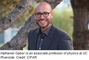
“It’s a bit like driving past a vineyard and looking out the window at the vineyard rows. Every now and then, you see no rows because you’re looking directly along a row,” said Nathaniel Gabor, an associate professor in the Department of Physics and Astronomy at the University of California, Riverside. “This is akin to what happens when two atomic layers are stacked on top of each other. At certain angles of twist, everything is energetically allowed. It adds up just right to allow for interesting possibilities of energy transfer.”
This is the future of new materials being synthesized by twisting and stacking atomically thin layers, and is still in the “alchemy” stage, Gabor added. To bring it all under one roof, he and physicist Justin C. W. Song of Nanyang Technological University, Singapore, have proposed this field of research be called “electron quantum metamaterials” and have just published a perspective article in Nature Nanotechnology.
“We highlight the potential of engineering synthetic periodic arrays with feature sizes below the wavelength of an electron. Such engineering allows the electrons to be manipulated in unusual ways, resulting in a new range of synthetic quantum metamaterials with unconventional responses,” Gabor said.
Metamaterials are a class of material engineered to produce properties that do not occur naturally. Examples include optical cloaking devices and super-lenses akin to the Fresnel lens that lighthouses use. Nature, too, has adopted such techniques—for example, in the unique coloring of butterfly wings—to manipulate photons as they move through nanoscale structures.
“Unlike photons that scarcely interact with each other, however, electrons in subwavelength structured metamaterials are charged, and they strongly interact,” Gabor said. “The result is an enormous variety of emergent phenomena and radically new classes of interacting quantum metamaterials.”
Gabor and Song were invited by Nature Nanotechnology to write a review paper. But the pair chose to delve deeper and lay out the fundamental physics that may explain much of the research in electron quantum metamaterials. They wrote a perspective paper instead that envisions the current status of the field and discusses its future.
“Researchers, including in our own labs, were exploring a variety of metamaterials but no one had given the field even a name,” said Gabor, who directs the Quantum Materials Optoelectronics lab at UCR. “That was our intent in writing the perspective. We are the first to codify the underlying physics. In a way, we are expressing the periodic table of this new and exciting field. It has been a herculean task to codify all the work that has been done so far and to present a unifying picture. The ideas and experiments have matured, and the literature shows there has been rapid progress in creating quantum materials for electrons. It was time to rein it all in under one umbrella and offer a road map to researchers for categorizing future work.”
In the perspective, Gabor and Song collect early examples in electron metamaterials and distil emerging design strategies for electronic control from them. They write that one of the most promising aspects of the new field occurs when electrons in subwavelength-structure samples interact to exhibit unexpected emergent behavior.
“The behavior of superconductivity in twisted bilayer graphene that emerged was a surprise,” Gabor said. “It shows, remarkably, how electron interactions and subwavelength features could be made to work together in quantum metamaterials to produce radically new phenomena. It is examples like this that paint an exciting future for electronic metamaterials. Thus far, we have only set the stage for a lot of new work to come.”
Share on:


Testimonial
"In a year when every marketing dollar mattered, I chose to keep I-Connect007 in our 2025 plan. Their commitment to high-quality, insightful content aligns with Koh Young’s values and helps readers navigate a changing industry. "
Brent Fischthal - Koh YoungSuggested Items
Sealed for Survival: Potting Electronics for the Toughest Environments
10/29/2025 | Beth Massey, MacDermid Alpha Electronics SolutionsElectronics deployed in harsh conditions face relentless threats from vibration, impact, chemical contaminants, airborne pollutants, and moisture, conditions that can quickly lead to failure without robust protection. Potting, the process of encapsulating electronics in a protective polymer, is a widely used strategy to safeguard devices from both environmental and mechanical hazards.
Driving Innovation: Mechanical and Optical Processes During Rigid-flex Production
10/28/2025 | Kurt Palmer -- Column: Driving InnovationRigid-flex printed circuit boards are a highly effective solution for placing complex circuitry in tight, three-dimensional spaces. They are now indispensable across a range of industries, from medical devices and aerospace to advanced consumer electronics, helping designers make the most efficient use of available space. However, their unique construction—combining rigid and flexible materials—presents a fundamental challenge for PCB manufacturers.
SMTAI 2025 Review: Reflecting on a Pragmatic and Forward-looking Industry
10/27/2025 | Marcy LaRont, I-Connect007Leaving the show floor on the final afternoon of SMTA International last week in Rosemont, Illinois, it was clear that the show remains a grounded, technically driven event that delivers a solid program, good networking, and an easy space to commune with industry colleagues and meet with customers.
ITW EAE Despatch Ovens Now Support ASTM 5423 Testing
10/15/2025 | ITW EAEAs the demand for high-performance electrical insulation materials continues to grow—driven by the rapid expansion of electric vehicles (EVs) and energy storage systems—thermal processing has become a critical step in material development.
Beyond Thermal Conductivity: Exploring Polymer-based TIM Strategies for High-power-density Electronics
10/13/2025 | Padmanabha Shakthivelu and Nico Bruijnis, MacDermid Alpha Electronics SolutionsAs power density and thermal loads continue to increase, effective thermal management becomes increasingly important. Rapid and efficient heat transfer from power semiconductor chip packages is essential for achieving optimal performance and ensuring long-term reliability of temperature-sensitive components. This is particularly crucial in power systems that support advanced applications such as green energy generation, electric vehicles, aerospace, and defense, along with high-speed computing for data centers and artificial intelligence (AI).