


 The Marketing Minute: Marketing With Layers
 The Right Approach: Electro-Tek—A Williams Family Legacy, Part 1
 It’s Only Common Sense: If You’re Not Differentiated, You’re Dead


New Materials: Growing Polymer Pelts
November 16, 2018 | KITEstimated reading time: 2 minutes
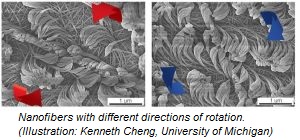
Polymer pelts made of the finest of fibers are suitable for many different applications, from coatings that adhere well and are easy to remove to highly sensitive biological detectors. Researchers at Karlsruhe Institute of Technology (KIT) together with scientists in the United States have now developed a cost-effective process to allow customized polymer nanofibers to grow on a solid substrate through vapor deposition of a liquid crystal layer with reactive molecules.
Surfaces with specially aligned fibers are quite abundant in nature and perform different functions such as sensing, adhering and self-cleaning. For example, the feet of geckos are covered with millions of hairs that allow them to adhere to surfaces and pull off again very easily. The synthesis of such surfaces from man-made materials opens up new perspectives for different applications. However, methods previously available for the production of polymer pelts on solid bases have been costly. What’s more important, the size, shape and alignment of the fibers can only be controlled to a limited extent with conventional methods.
Researchers at the Institute of Functional Interfaces (IFG) of KIT, as well as at the University of Michigan, the University of Wisconsin-Madison and Cornell University in Ithaca, New York, have now developed a simple and therefore cost-effective process that allows polymer pelts to grow in a self-organized way. The research group led by Professor Joerg Lahann, Head of the Department of New Polymers and Biomaterials at KIT’s IFG and Director of the Biointerfaces Institute of the University of Michigan, present the new process in the journal Science. First of all, they cover a carrier with a thin layer of liquid crystals, which are substances that are liquid, have directional properties and are otherwise used especially for screens and displays (liquid crystal displays – LCDs). Next, the liquid crystal layer is exposed to activated molecules by vapor deposition. These reactive monomers penetrate the liquid crystalline layer and grow from the substrate into the liquid in the form of fine fibers.
As a result, polymer nanofibers are created that can be customized in length, diameter, shape and arrangement. The complex but precisely structured polymer pelts formed by the fibers are attractive for many different applications, especially for biological detectors, bioinstructive surfaces that interact with their environment, and for coatings with new properties. This also includes surfaces with dry adhesion properties similar to those of gecko feet, although adhesion in nanofibers is based on a special spatial arrangement of the atoms in the molecules (chirality – handedness).
The German Research Foundation (DFG) funded the work at the “Molecular Structuring of Soft Matter” Collaborative Research Center (CRC). In the 3D Matter Made to Order (3DMM2O) cluster of KIT and the University of Heidelberg, which will be funded in the Excellence Strategy by the federal and state governments from January 2019, the focus will also be on customized materials. The 3DMM2O Excellence Cluster, in which the Head of KIT’s IFG, Professor Christof Wöll, is involved as one of the main researchers, combines natural and engineering sciences, focusing on three-dimensional additive production technologies from a molecular to macroscopic level.
Share on:


Testimonial
"The I-Connect007 team is outstanding—kind, responsive, and a true marketing partner. Their design team created fresh, eye-catching ads, and their editorial support polished our content to let our brand shine. Thank you all! "
Sweeney Ng - CEE PCBSuggested Items
The Marketing Minute: Marketing With Layers
10/15/2025 | Brittany Martin -- Column: The Marketing MinuteMarketing to a technical audience is like crafting a multilayer board: Each layer serves a purpose, from the surface story to the buried detail that keeps everything connected. At I-Connect007, we’ve learned that the best marketing campaigns aren’t built linearly; they’re layered. A campaign might start with a highly technical resource, such as an in-depth article, a white paper, or a podcast featuring an engineer delving into the details of a process. That’s the foundation, the substance that earns credibility.
Taking Control of PCB Verification One Step at a Time
10/09/2025 | Kirk Fabbri, Siemens EDAToday’s designs are as complex as ever, and engineers face tough decisions every day. Simulation and verification teams are confronted with a three-fold challenge: understanding the underlying theory, mastering the tools, and applying best practices.Engineers need to navigate a vast and ever-changing cast of design and simulation tools, often with overlapping functionality.
Happy’s Tech Talk #43: Engineering Statistics Training With Free Software
10/06/2025 | Happy Holden -- Column: Happy’s Tech TalkIn over 50 years as a PCB process engineer, the one skill I acquired in college that has been most beneficial is engineering statistics. Basic statistics was part of my engineering fundamentals classes, but I petitioned the dean to let me take the engineering statistics graduate course because I was creating a senior thesis for my honors focus and needed more training on Design of Experiments (DOE).
Connect the Dots: Evolution of PCB Manufacturing—Lamination
10/02/2025 | Matt Stevenson -- Column: Connect the DotsWhen I wrote The Printed Circuit Designer's Guide to...™ Designing for Reality, it was not a one-and-done effort. Technology is advancing rapidly. Designing for the reality of PCB manufacturing will continue to evolve. That’s why I encourage designers to stay on top of the tools and processes used during production, to ensure their designs capitalize on the capabilities of their manufacturing partner.
Empower Sets New Benchmark with 20x Faster Response and Breakthrough Sustainability Demonstrated at OCP Global Summit 2025
09/25/2025 | Empower SemiconductorEmpower Semiconductor, the world leader in powering AI-class processors, announced that its Crescendo chipset, an artificial intelligence (AI) and high-performance computing (HPC) processor true vertical power delivery platform, is available now for final sampling, with mass production slated for late 2025.