


 The Marketing Minute: Marketing With Layers
 The Right Approach: Electro-Tek—A Williams Family Legacy, Part 1
 It’s Only Common Sense: If You’re Not Differentiated, You’re Dead


Photonic Radiation Sensors Survive Huge Doses Undamaged
November 28, 2018 | NISTEstimated reading time: 4 minutes
Researchers at the National Institute of Standards and Technology (NIST) have published landmark test results that suggest a promising class of sensors can be used in high-radiation environments and to advance important medical, industrial and research applications.
Photonic sensors convey information with light instead of electric currents in wires. They can measure, transmit and manipulate streams of photons, typically through optical fibers, and are used to gauge pressure, temperature, distance, magnetic fields, environmental conditions and more.
They are attractive because of their small size, low power consumption and tolerance of environmental variables such as mechanical vibration. But the general consensus has been that high levels of radiation would modify the optical properties of their silicon, leading to incorrect readings.
So NIST, long a world leader in many areas of photonics research, launched a program to answer those questions. The test results indicate the sensors could be customized for measuring radiation dose in both industrial applications and clinical radiotherapy.
Specifically, the NIST results suggest the sensors could be used to track levels of ionizing radiation (with energy high enough to alter the structure of atoms) used in food irradiation to destroy microbes and in medical device sterilization—estimated to be a $7 billion annual market in the U.S. alone. The sensors also have potential applications in medical imaging and therapy, which together are projected to total nearly $50 billion in annual value worldwide by 2022.
“When we looked at publications on the subject, different labs were getting dramatically different results,” said project scientist Zeeshan Ahmed, who is part of NIST’s Photonic Dosimetry Project and leader of NIST’s cutting-edge Photonic Thermometry Project. “That was our main motivation for doing our experiment.”
“Another motivation was the growing interest in deploying photonic sensors that can function accurately in very harsh environments, such as close to nuclear reactors, where radiation damage is a major concern,” Ahmed said.
“In addition, the space industry needs to know how these devices would function in high-radiation environments,” said project scientist Ronald Tosh. “Are they going to get damaged or not? What this study shows is that for a certain class of devices and radiation, the damage is negligible.”
“We found that oxide-coated silicon photonic devices can withstand radiation exposure up to 1 million gray,” said Photonic Dosimetry project leader Ryan Fitzgerald, using the SI unit for absorbed radiation. One gray represents one joule of energy absorbed by one kilogram of mass, and 1 gray corresponds to 10,000 chest X-rays. This is roughly what a sensor would receive at a nuclear power plant.
“It’s the upper limit of what our calibrations customers care about,” Fitzgerald said. “So the devices can be assumed to work reliably at industrial or medical radiation levels that are hundreds or thousands of times lower.” Food irradiation, for example, ranges from a few hundred to a few thousand gray, and is typically monitored by its effects on pellets of alanine, an amino acid that changes its atomic properties when exposed to ionizing radiation.
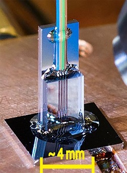
To determine the effects of radiation, the NIST researchers exposed two kinds of silicon photonic sensors to hours of gamma radiation from cobalt-60, a radioactive isotope. In both types of sensors, small variations in their physical properties change the wavelength of the light that travels through them. By measuring those changes, the devices can be used as highly sensitive thermometers or strain gauges. This remains true in extreme environments like space flight or nuclear reactors, only if they continue to function properly under exposure to ionizing radiation.
“Our results show that these photonic devices are robust in even extreme radiation environments, which suggests they could be also used to measure radiation via its effects on physical properties of irradiated devices,” Fitzgerald said. “That should come as good news for U.S. manufacturing, which is anxious to serve the large and growing market for precise delivery of radiation at very small length scales. Photonic sensors could then be developed to measure low-energy electron and X-ray beams used in medical device sterilization and food irradiation.”
They will also be of great interest to clinical medicine, in which physicians strive to treat cancers and other conditions with the lowest effective levels of radiation focused on the smallest dimensions to avoid affecting healthy tissue, including electron, proton and ion beams.
Reaching that goal demands radiation sensors with extraordinarily high sensitivity and spatial resolution. “Eventually, we hope to develop chip-scale devices for industrial and medical applications that can determine absorbed dose gradients over distances in the range of micrometers and thus provide unprecedented detail in measurements,” said project scientist Nikolai Klimov. A micrometer is a millionth of a meter. A human hair is about 100 micrometers wide.
The team’s results may have large implications for new medical therapies that employ extremely narrow beams of protons or carbon ions and medical sterilization processes that use low-energy beams of electrons. “Our sensors are naturally small and chip-scale,” Fitzgerald said. “Current dosimeters are on the order of millimeters to centimeters, which can give erroneous readings for fields that vary over those dimensions.”
In the next stage of the research, the team will test arrays of sensors simultaneously in identical conditions to see if variations in dose over small distances can be resolved.
Share on:


Testimonial
"Our marketing partnership with I-Connect007 is already delivering. Just a day after our press release went live, we received a direct inquiry about our updated products!"
Rachael Temple - AlltematedSuggested Items
Smart Eye Collaborates with Sony on Next-Generation Interior Sensing and Iris Authentication
10/09/2025 | Smart EyeSmart Eye AB, the global leader in Interior Sensing AI and Driver Monitoring Systems (DMS), announced a collaboration with Sony Semiconductor Solutions Corporation (Sony) to integrate Smart Eye’s interior sensing and biometric authentication software with Sony’s newly released IMX775 RGB-IR image sensor.
SEMICON Europa 2025 to Highlight Innovations in Advanced Packaging, Fab Management, and MEMS and Imaging Sensors to Bolster Europe’s Semiconductor Resilience
10/03/2025 | SEMISemiconductor industry experts will convene at SEMICON Europa 2025, November 18-21 at Messe München in Munich, to explore the latest trends and innovations in advanced packaging and fab management.
MEMS & Imaging Sensors Summit to Spotlight Sensing Revolution for Europe’s Leadership
09/11/2025 | SEMIIndustry experts will gather November 19-20 at the SEMI MEMS & Imaging Sensors Summit 2025 to explore the latest breakthroughs in AI-driven MEMS and imaging optimization, AR/VR technologies, and advanced sensor solutions for critical defence applications.
Direct Imaging System Market Size to Hit $4.30B by 2032, Driven by Increasing Demand for High-Precision PCB Manufacturing
09/11/2025 | Globe NewswireAccording to the SNS Insider, “The Direct Imaging System Market size was valued at $2.21 Billion in 2024 and is projected to reach $4.30 Billion by 2032, growing at a CAGR of 8.68% during 2025-2032.”
I-Connect007’s Editor’s Choice: Five Must-Reads for the Week
07/04/2025 | Marcy LaRont, I-Connect007For our industry, we have seen several bullish market announcements over the past few weeks, including one this week by IDC on the massive growth in the global server market. We’re also closely watching global trade and nearshoring. One good example of successful nearshoring is Rehm Thermal Systems, which celebrates its 10th anniversary in Mexico and the official opening of its new building in Guadalajara.