


 The Marketing Minute: Marketing With Layers
 The Right Approach: Electro-Tek—A Williams Family Legacy, Part 1
 It’s Only Common Sense: If You’re Not Differentiated, You’re Dead


New Device Widens Light Beams by 400 Times
November 29, 2018 | NISTEstimated reading time: 2 minutes
By using light waves instead of electric current to transmit data, photonic chips—circuits for light—have advanced fundamental research in many areas from timekeeping to telecommunications. But for many applications, the narrow beams of light that traverse these circuits must be substantially widened in order to connect with larger, off-chip systems. Wider light beams could boost the speed and sensitivity of medical imaging and diagnostic procedures, security systems that detect trace amounts of toxic or volatile chemicals and devices that depend on the analysis of large groupings of atoms.
Scientists at the National Institute of Standards and Technology (NIST) have now developed a highly efficient converter that enlarges the diameter of a light beam by 400 times. NIST physicist Vladimir Aksyuk and his colleagues, including researchers from the University of Maryland NanoCenter in College Park, Maryland, and Texas Tech University in Lubbock, described their work in the journal Light: Science and Applications.
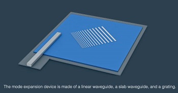
The converter widens the cross section, or area of the beam, in two consecutive stages. Initially, the light travels along an optical waveguide —a thin, transparent channel whose optical properties limit the diameter of the beam to a few hundred nanometers, less than one-thousandth the average diameter of a human hair. Because the waveguide channel is so narrow, some of the traveling light extends outward beyond the edges of the waveguide. Taking advantage of this broadening, the team placed a rectangular slab composed of the same material as the waveguide a tiny, precisely measured distance from the waveguide. The light can jump across the tiny gap between the two components and gradually leak into the slab.
The slab maintains the narrow width of the light in the vertical (top-to-bottom) dimension, but it provides no such constraints for the lateral, or sideways, dimension. As the gap between the waveguide and the slab is gradually changed, the light in the slab forms a precisely directed beam 400 times wider than the approximately 300 nm diameter of the original beam.
In the second stage of the expansion, which enlarges the vertical dimension of the light, the beam traveling through the slab encounters a diffraction grating. This optical device has periodic rulings or lines, each of which scatters light. The team designed the depth and spacing of the rulings to vary so that the light waves combine, forming a single wide beam directed at nearly a right angle to the chip’s surface.
Importantly, the light remains collimated, or precisely parallel, throughout the two-stage expansion process, so that it stays on target and does not spread out. The area of the collimated beam is now large enough to travel the long distance needed to probe the optical properties of large diffuse groupings of atoms.
Working with a team led by John Kitching of NIST in Boulder, Colorado, the researchers have already used the two-stage converter to successfully analyze the properties of some 100 million gaseous rubidium atoms as they jumped from one energy level to another. That’s an important proof-of-concept because devices based on interactions between light and atomic gasses can measure quantities such as time, length and magnetic fields and have applications in navigation, communications and medicine.
“Atoms move very quickly, and if the beam monitoring them is too small, they move in and out of the beam so fast that it becomes difficult to measure them,” said Kitching. “With large laser beams, the atoms stay in the beam for longer and allow for more precise measurement of the atomic properties,” he added. Such measurements could lead to improved wavelength and time standards.
Share on:


Testimonial
"In a year when every marketing dollar mattered, I chose to keep I-Connect007 in our 2025 plan. Their commitment to high-quality, insightful content aligns with Koh Young’s values and helps readers navigate a changing industry. "
Brent Fischthal - Koh YoungSuggested Items
Smart Eye Collaborates with Sony on Next-Generation Interior Sensing and Iris Authentication
10/09/2025 | Smart EyeSmart Eye AB, the global leader in Interior Sensing AI and Driver Monitoring Systems (DMS), announced a collaboration with Sony Semiconductor Solutions Corporation (Sony) to integrate Smart Eye’s interior sensing and biometric authentication software with Sony’s newly released IMX775 RGB-IR image sensor.
SEMICON Europa 2025 to Highlight Innovations in Advanced Packaging, Fab Management, and MEMS and Imaging Sensors to Bolster Europe’s Semiconductor Resilience
10/03/2025 | SEMISemiconductor industry experts will convene at SEMICON Europa 2025, November 18-21 at Messe München in Munich, to explore the latest trends and innovations in advanced packaging and fab management.
MEMS & Imaging Sensors Summit to Spotlight Sensing Revolution for Europe’s Leadership
09/11/2025 | SEMIIndustry experts will gather November 19-20 at the SEMI MEMS & Imaging Sensors Summit 2025 to explore the latest breakthroughs in AI-driven MEMS and imaging optimization, AR/VR technologies, and advanced sensor solutions for critical defence applications.
Direct Imaging System Market Size to Hit $4.30B by 2032, Driven by Increasing Demand for High-Precision PCB Manufacturing
09/11/2025 | Globe NewswireAccording to the SNS Insider, “The Direct Imaging System Market size was valued at $2.21 Billion in 2024 and is projected to reach $4.30 Billion by 2032, growing at a CAGR of 8.68% during 2025-2032.”
I-Connect007’s Editor’s Choice: Five Must-Reads for the Week
07/04/2025 | Marcy LaRont, I-Connect007For our industry, we have seen several bullish market announcements over the past few weeks, including one this week by IDC on the massive growth in the global server market. We’re also closely watching global trade and nearshoring. One good example of successful nearshoring is Rehm Thermal Systems, which celebrates its 10th anniversary in Mexico and the official opening of its new building in Guadalajara.