


 The Marketing Minute: Marketing With Layers
 The Right Approach: Electro-Tek—A Williams Family Legacy, Part 1
 It’s Only Common Sense: If You’re Not Differentiated, You’re Dead


Merging Memory and Computation, Programmable Chip Speeds AI, Slashes Power Use
November 30, 2018 | Princeton UniversityEstimated reading time: 4 minutes
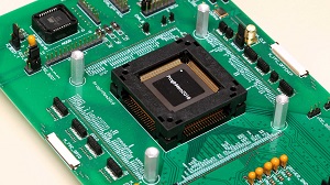
By shifting a fundamental property of computation, Princeton researchers have built a new type of computer chip that boosts the performance and slashes the energy demands of systems used for artificial intelligence.
The chip, which works with standard programming languages, could be particularly useful on phones, watches or other devices that rely on high-performance computing and have limited battery life.
The chip, based on a technique called in-memory computing, is designed to clear a primary computational bottleneck that forces computer processors to expend time and energy fetching data from stored memory. In-memory computing performs computation directly in the storage, allowing for greater speed and efficiency.
The announcement of the new chip, along with a system to program it, follows closely on an earlier report that the researchers in collaboration with Analog Devices Inc. had fabricated circuitry for in-memory computing. Lab tests of the circuitrydemonstrated that the chip would perform tens to hundreds of times faster than comparable chips. However, the initial chip did not include all the components of the most recent version, so its capability was limited.
In the new announcement, researchers in the lab of Naveen Verma, an associate professor of electrical engineering, report that they have integrated the in-memory circuitry into a programmable processor architecture. The chip now works with common computer languages such as C.
“The previous chip was a strong and powerful engine,” said Hongyang Jia, a graduate student in Verma’s group and one of the chip designers. “This chip is the whole car.”
Although it could operate with a broad range of systems, the Princeton chip is intended to support systems designed for deep-learning inference — algorithms that allow computers to make decisions and perform complex tasks by learning from data sets. Deep learning systems direct such things as self-driving cars, facial recognition systems and medical diagnostic software.
Verma said that for many applications, the chip’s energy savings would be as critical as the performance boost. That is because many AI applications are expected to operate on devices driven by batteries such as mobile phones or wearable medical sensors. The Apple iPhone X, for example, already has an AI chip as part of its circuitry. But, both the energy savings and performance boosts are only of use if they can be accessed by the broad base of applications that need them — that is where the need for programmability comes in.
“The classic computer architecture separates the central processor, which crunches the data, from the memory, which stores the data,” Verma said. “A lot of the computer’s energy is used in moving data back and forth.”
In part, the new chip is a response to the slowing promise of Moore’s Law. In 1965, Intel founder Gordon Moore observed that the number of transistors on integrated circuits doubled about every year, and the industry also noted that those transistors became faster and more energy efficient in the process. For decades, these observations, which became known as Moore’s Law, underpinned a transformation in which computers became ever more powerful. But in recent years, transistors have not kept improving as in the past, running into fundamental limitations of their physics.
Verma, who specializes in circuit and system design, thought about ways around this squeeze on the architectural level rather than the transistor level. The computation needed by AI would be much more efficient if it could be done at the same location as the computer’s memory because it would eliminate the time and energy used to fetch data stored far away. That would make the computer faster without upgrading the transistors. But creating such a system posed a challenge. Memory circuits are designed as densely as possible in order to pack in large amounts of data. Computation, on the other hand, requires that space be devoted for additional transistors.
One option was to substitute electrical components called capacitors for the transistors. Transistors are essentially switches that use voltage changes to stand for the 1s and 0s that make up binary computer signals. They can do all sorts of calculations using arrays of 1 and 0 digits, which is why the systems are called digital. Capacitors store and release electrical charge, so they can represent any number, not just 1s and 0s. Verma realized that with capacitors he could perform calculations in a much denser space than he could with transistors.
Capacitors also can be made very precisely on a chip, much more so than transistors. The new design pairs capacitors with conventional cells of static random access memory (SRAM) on a chip. The combination of capacitors and SRAM is used to perform computations on the data in the analog (not digital) domain, yet in ways that are reliable and amenable to including programmability features. Now, the memory circuits can perform calculations in ways directed by the chip’s central processing unit.
“In-memory computing has been showing a lot of promise in recent years, in really addressing the energy and speed of computing systems,” said Verma. “But the big question has been whether that promise would scale and be usable by system designers towards all of the AI applications we really care about. That makes programmability necessary.”
In addition to Verma and Jia, authors of the paper include Yinqi Tang, Hossein Valavi and Jintao Zhang, all graduate students in electrical engineering. Support for the research was provided in part by Analog Devices Inc.
Share on:


Testimonial
"The I-Connect007 team is outstanding—kind, responsive, and a true marketing partner. Their design team created fresh, eye-catching ads, and their editorial support polished our content to let our brand shine. Thank you all! "
Sweeney Ng - CEE PCBSuggested Items
TI’s New Power-management Solutions Enable Scalable AI Infrastructures
10/14/2025 | Texas InstrumentsTexas Instruments (TI) debuted new design resources and power-management chips to help companies meet growing artificial intelligence (AI) computing demands and scale power-management architectures from 12V to 48V to 800 VDC.
Yamaha Boosts Surface-Mount Programming Efficiency with Latest Software Release
10/14/2025 | Yamaha Robotics SMT SectionYamaha Robotics SMT Section has introduced enhanced software tools to accelerate new product introduction (NPI) using YSUP-PG, the program generator for the company’s surface-mounters and inspection systems.
Western Digital Opens Expanded System Integration Test Lab to Accelerate Innovation in the AI and Cloud Era
10/14/2025 | BUSINESS WIREWestern Digital, the backbone of the AI-driven data economy, announced the opening of its expanded System Integration and Test (SIT) Lab, a state-of-the-art 25,600 square foot facility designed to accelerate customer success and unlock faster time to value.
Wiley Launches Interoperable Platform to Power Scientific Discovery in World's Leading AI Technologies
10/14/2025 | BUSINESS WIREWiley, a global leader in authoritative content and research intelligence, announced the launch of Wiley AI Gateway, the industry's first AI-native research intelligence platform that provides researchers access to trusted content from world-leading scholarly publishers through a single endpoint.
Momentus Signs $15 Million Global Agreement with Solstar Space
10/14/2025 | BUSINESS WIREMomentus Inc., a commercial space firm specializing in satellite solutions and in-space infrastructure, announced a three-year reciprocal services agreement with Solstar Space (Solstar).