


 The Marketing Minute: Marketing With Layers
 The Right Approach: Electro-Tek—A Williams Family Legacy, Part 1
 It’s Only Common Sense: If You’re Not Differentiated, You’re Dead


Switching Identities: Revolutionary Insulator-Like Material Also Conducts Electricity
November 30, 2018 | University of Wisconsin–MadisonEstimated reading time: 3 minutes
University of Wisconsin–Madison researchers have made a material that can transition from an electricity-transmitting metal to a nonconducting insulating material without changing its atomic structure.
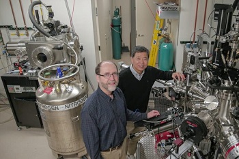
Image Caption: Chang-Beom Eom, right, and Mark Rzchowski inspect a materials growth chamber. The researchers have made a new material that can be switched from electrical conductor to insulator. UW–Madison photo by Sam Million-Weaver
“This is quite an exciting discovery,” says Chang-Beom Eom, professor of materials science and engineering. “We’ve found a new method of electronic switching.”
The new material could lay the groundwork for ultrafast electronic devices, such as the cellphones and computers of the future.
Metals like copper or silver conduct electricity, whereas insulators like rubber or glass do not allow current to flow. Some materials, however, can transition from insulating to conducting and back again.
This transition usually means that the arrangement of a material’s atoms and its conducting electrons must change in a coordinated way, but the atomic transition typically proceeds much more slowly than the smaller, lighter electrons that conduct electricity.
A material that can switch to conducting electricity like a metal without moving its atoms could dramatically advance switching speeds of advanced devices, says Eom.
“The metal-to-insulator transition is very important for switches and for logic devices with a one or a zero state,” he says. “We have the potential to use this concept to make very fast switches.”
In their research, Eom and his collaborators answered a fundamental question that has bothered scientists for years: Can the electronic and structural transition be decoupled — essentially, can the quickly changing electrons break out on their own and leave the atoms behind?
They used a material called vanadium dioxide, which is a metal when it’s heated and an insulator when it’s at room temperature. At high temperatures, the atoms that make up vanadium dioxide are arranged in a regularly repeating pattern that scientists refer to as the rutile phase. When vanadium dioxide cools down to become an insulator, its atoms adopt a different pattern, called monoclinic.
No naturally occurring substances conduct electricity when their atoms are in the monoclinic conformation. And it takes time for the atoms to rearrange when a material reaches the insulator-to-metal transition temperature.
Crucially, vanadium dioxide transitions between a metal and an insulator at different temperatures depending upon the amount of oxygen present in the material. The researchers leveraged that fact to create two thin layers of vanadium dioxide — one with a slightly lower transition temperature than the other — sandwiched on top of each other, with a sharp interface between.
When they heated the thin vanadium dioxide sandwich, one layer made the structural switch to become a metal. Atoms in the other layer remained locked into the insulating monoclinic phase. Surprisingly, however, that part of the material conducted electricity.
The new material could lay the groundwork for ultrafast electronic devices, such as the cellphones and computers of the future.
Most importantly, the material remained stable and retained its unique characteristics.
Although other research groups have attempted to create electrically conductive insulators, those materials lost their properties almost instantly — persisting for mere femtoseconds, or a few thousandths of one trillionth of a second.
The Eom team’s material, however, is here to stay.
“We were able to stabilize it, making it useful for real devices,” says Eom.
Key to their approach was the dual-layer, sandwich structure. Each layer was so thin that the interface between the two materials dominated how the entire stack behaved. It’s a notion that Eom and colleagues plan to pursue further.
“Designing interfaces could open up new materials,” says Eom.
The Wisconsin Alumni Research Foundation is assisting the researchers with patent filing.
Share on:


Testimonial
"Advertising in PCB007 Magazine has been a great way to showcase our bare board testers to the right audience. The I-Connect007 team makes the process smooth and professional. We’re proud to be featured in such a trusted publication."
Klaus Koziol - atgSuggested Items
Episode 6 of Ultra HDI Podcast Series Explores Copper-filled Microvias in Advanced PCB Design and Fabrication
10/15/2025 | I-Connect007I-Connect007 has released Episode 6 of its acclaimed On the Line with... American Standard Circuits: Ultra High Density Interconnect (UHDI) podcast series. In this episode, “Copper Filling of Vias,” host Nolan Johnson once again welcomes John Johnson, Director of Quality and Advanced Technology at American Standard Circuits, for a deep dive into the pros and cons of copper plating microvias—from both the fabricator’s and designer’s perspectives.
Nolan’s Notes: Tariffs, Technologies, and Optimization
10/01/2025 | Nolan Johnson -- Column: Nolan's NotesLast month, SMT007 Magazine spotlighted India, and boy, did we pick a good time to do so. Tariff and trade news involving India was breaking like a storm surge. The U.S. tariffs shifted India from one of the most favorable trade agreements to the least favorable. Electronics continue to be exempt for the time being, but lest you think that we’re free and clear because we manufacture electronics, steel and aluminum are specifically called out at the 50% tariff levels.
MacDermid Alpha & Graphic PLC Lead UK’s First Horizontal Electroless Copper Installation
09/30/2025 | MacDermid Alpha & Graphic PLCMacDermid Alpha Electronics Solutions, a leading supplier of integrated materials and chemistries to the electronics industry, is proud to support Graphic PLC, a Somacis company, with the installation of the first horizontal electroless copper metallization process in the UK.
Electrodeposited Copper Foils Market to Grow by $11.7 Billion Over 2025-2032
09/18/2025 | Globe NewswireThe global electrodeposited copper foils market is poised for dynamic growth, driven by the rising adoption in advanced electronics and renewable energy storage solutions.
MacDermid Alpha Showcases Advanced Interconnect Solutions at PCIM Asia 2025
09/18/2025 | MacDermid Alpha Electronics SolutionsMacDermid Alpha Electronic Solutions, a global leader in materials for power electronics and semiconductor assembly, will showcase its latest interconnect innovations in electronic interconnect materials at PCIM Asia 2025, held from September 24 to 26 at the Shanghai New International Expo Centre, Booth N5-E30