


 The Marketing Minute: Marketing With Layers
 The Right Approach: Electro-Tek—A Williams Family Legacy, Part 1
 It’s Only Common Sense: If You’re Not Differentiated, You’re Dead


New Quantum Materials Could Take Computers Beyond the Semiconductor Era
December 4, 2018 | UC BerkeleyEstimated reading time: 5 minutes
Researchers from Intel Corp. and UC Berkeley are looking beyond current transistor technology and preparing the way for a new type of memory and logic circuit that could someday be in every computer on the planet.
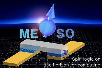
Image Caption: MESO devices, based on magnetoelectric and spin-orbit materials, could someday replace the ubiquitous semiconductor transistor, today represented by CMOS. MESO uses up-and-down magnetic spins in a multiferroic material to store binary information and conduct logic operations. (Intel graphic)
In a paper appearing online Dec. 3 in advance of publication in the journal Nature, the researchers propose a way to turn relatively new types of materials, multiferroics and topological materials, into logic and memory devices that will be 10 to 100 times more energy-efficient than foreseeable improvements to current microprocessors, which are based on CMOS (complementary metal–oxide–semiconductor).
The magneto-electric spin-orbit or MESO devices will also pack five times more logic operations into the same space than CMOS, continuing the trend toward more computations per unit area, a central tenet of Moore’s Law.
The new devices will boost technologies that require intense computing power with low energy use, specifically highly automated, self-driving cars and drones, both of which require ever increasing numbers of computer operations per second.
“As CMOS develops into its maturity, we will basically have very powerful technology options that see us through. In some ways, this could continue computing improvements for another whole generation of people,” said lead author Sasikanth Manipatruni, who leads hardware development for the MESO project at Intel’s Components Research group in Hillsboro, Oregon. MESO was invented by Intel scientists, and Manipatruni designed the first MESO device.
Transistor technology, invented 70 years ago, is used today in everything from cellphones and appliances to cars and supercomputers. Transistors shuffle electrons around inside a semiconductor and store them as binary bits 0 and 1.
Single crystals of the multiferroic material bismuth-iron-oxide. The bismuth atoms (blue) form a cubic lattice with oxygen atoms (yellow) at each face of the cube and an iron atom (gray) near the center. The somewhat off-center iron interacts with the oxygen to form an electric dipole (P), which is coupled to the magnetic spins of the atoms (M) so that flipping the dipole with an electric field (E) also flips the magnetic moment. The collective magnetic spins of the atoms in the material encode the binary bits 0 and 1, and allow for information storage and logic operations.
In the new MESO devices, the binary bits are the up-and-down magnetic spin states in a multiferroic, a material first created in 2001 by Ramamoorthy Ramesh, a UC Berkeley professor of materials science and engineering and of physics and a senior author of the paper.
“The discovery was that there are materials where you can apply a voltage and change the magnetic order of the multiferroic,” said Ramesh, who is also a faculty scientist at Lawrence Berkeley National Laboratory. “But to me, ‘What would we do with these multiferroics?’ was always a big question. MESO bridges that gap and provides one pathway for computing to evolve”.
In the Nature paper, the researchers report that they have reduced the voltage needed for multiferroic magneto-electric switching from 3 volts to 500 millivolts, and predict that it should be possible to reduce this to 100 millivolts: one-fifth to one-tenth that required by CMOS transistors in use today. Lower voltage means lower energy use: the total energy to switch a bit from 1 to 0 would be one-tenth to one-thirtieth of the energy required by CMOS.
“A number of critical techniques need to be developed to allow these new types of computing devices and architectures,” said Manipatruni, who combined the functions of magneto-electrics and spin-orbit materials to propose MESO. “We are trying to trigger a wave of innovation in industry and academia on what the next transistor-like option should look like.”
Page 1 of 2
Share on:


Testimonial
"In a year when every marketing dollar mattered, I chose to keep I-Connect007 in our 2025 plan. Their commitment to high-quality, insightful content aligns with Koh Young’s values and helps readers navigate a changing industry. "
Brent Fischthal - Koh YoungSuggested Items
ITW EAE Despatch Ovens Now Support ASTM 5423 Testing
10/15/2025 | ITW EAEAs the demand for high-performance electrical insulation materials continues to grow—driven by the rapid expansion of electric vehicles (EVs) and energy storage systems—thermal processing has become a critical step in material development.
Beyond Thermal Conductivity: Exploring Polymer-based TIM Strategies for High-power-density Electronics
10/13/2025 | Padmanabha Shakthivelu and Nico Bruijnis, MacDermid Alpha Electronics SolutionsAs power density and thermal loads continue to increase, effective thermal management becomes increasingly important. Rapid and efficient heat transfer from power semiconductor chip packages is essential for achieving optimal performance and ensuring long-term reliability of temperature-sensitive components. This is particularly crucial in power systems that support advanced applications such as green energy generation, electric vehicles, aerospace, and defense, along with high-speed computing for data centers and artificial intelligence (AI).
Is Glass Finally Coming of Age?
10/13/2025 | Nolan Johnson, I-Connect007Substrates, by definition, form the base of all electronic devices. Whether discussing silicon wafers for semiconductors, glass-and-epoxy materials in printed circuits, or the base of choice for interposers, all these materials function as substrates. While other substrates have come and gone, silicon and FR-4 have remained the de facto standards for the industry.
Creative Materials to Showcase Innovative Functional Inks for Medical Devices at COMPAMED 2025
10/09/2025 | Creative Materials, Inc.Creative Materials, a leading manufacturer of high-performance functional inks and coatings, is pleased to announce its participation in COMPAMED 2025, taking place November 17–20 in Düsseldorf, Germany.
Jiva Leading the Charge Toward Sustainable Innovation
09/30/2025 | Marcy LaRont, PCB007 MagazineEnvironmental sustainability in business—product circularity—is a high priority these days. “Circularity,” the term meant to replace “recycling,” in its simplest definition, describes a full circle life for electronic products and all their elements. The result is re-use or a near-complete reintroduction of the base materials back into the supply chain, leaving very little left for waste. For what cannot be reused productively, the ultimate hope is to have better, less harmful means of disposal and/or materials that can seamlessly and harmlessly decompose and integrate back into the natural environment. That is where Jiva and Soluboard come in.