


 The Marketing Minute: Marketing With Layers
 The Right Approach: Electro-Tek—A Williams Family Legacy, Part 1
 It’s Only Common Sense: If You’re Not Differentiated, You’re Dead


Better Biomedical Devices, Wearable Displays May Result From Tiny Light-Guiding Structures
December 17, 2018 | OSAEstimated reading time: 3 minutes
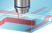
For the first time, researchers have fabricated light-guiding structures known as waveguides just over one micron wide in a clear silicone commonly used for biomedical applications. The tiny, flexible waveguides can be used to make light-based devices such as biomedical sensors and endoscopes that are smaller and more complex than currently possible.
Image Caption: Researchers optimized a laser writing process to create extremely narrow waveguides in a type of silicone known as PDMS. The new waveguides could be used to transport light in a variety of sensors, lab-on-a-chip systems and wearable devices. Credit: Ye Pu, École Fédérale de Lausanne.
“To the best of our knowledge, these are the smallest optical waveguides ever created in polydimethylsiloxane, or PDMS,” said research team member Ye Pu of École Fédérale de Lausanne in Switzerland. “Our flexible waveguides could be integrated into microfluidic lab-on-a-chip systems to eliminate bulky external optics needed to perform blood tests, for example. They might also deliver light for wearable devices such as a shirt featuring a display.”
As reported in the journal Optical Materials Express, the new optical waveguides are not only thinner than a piece of dust, they also exhibit very low light loss when used with certain wavelengths of light. A light-based signal can travel through the new waveguides for 10 centimeters or more before an unacceptable degradation of the signal will occur.
Creating Structures with Light
The researchers made the new waveguides by optimizing laser direct writing, a microfabrication approach that creates detailed 3-D structures by polymerizing a light sensitive chemical with a precisely positioned focused laser. Polymerization converts relatively small molecules called monomers into large, chainlike polymers.
The new approach does not require a photoinitiator, which is typically used to efficiently absorb the laser light and convert it into chemical energy that initiates polymerization. “By not using a photoinitiator, we simplified the fabrication process and also enhanced the compatibility of the final device with living tissue,” Pu said. “This enhanced biocompatibility could allow the approach to be used to make implantable sensors and devices.”
The new flexible waveguides could also serve as building blocks for photonic printed circuit boards that use high-speed optical signals rather than electrical links to transmit data in computers and other electronic devices.
Confining the Light
To achieve a small optical waveguide that efficiently confines light, there must be a large difference between the refractive index of the material making up the waveguides and the surrounding PDMS. The researchers used phenylacetylene for the waveguides because, compared to traditionally used materials, it has a higher refractive index once polymerized. As an added benefit, it also can be easily loaded into PDMS simply by soaking the PDMS in liquid phenylacetylene.
After soaking the PDMS in phenylacetylene, the researchers used focused ultrafast laser pulses to induce an optical phenomenon known as multiphoton absorption in which multiple photons are absorbed at once. Multiphoton laser direct writing produces much finer structures than one-photon processes because the volume of polymerization at each writing spot is much smaller. Using multiphoton laser direct writing also allowed the researchers to directly initiate phenylacetylene polymerization without a photoinitiator. They then evaporated any unpolymerized phenylacetylene by heating the PDMS.
The researchers showed that this new approach could make flexible waveguides in PDMS that are just 1.3 microns wide. For the 650 to 700 nanometer spectral band, only 0.07% of the light transmitted through the waveguides is lost every centimeter. Optimizing the setup would likely allow fabrication of waveguides that are smaller than 1 micron, according to the researchers.
A Flexible Endoscope
The researchers are now working to improve the yield of the fabrication process by developing a control system that would help avoid material damage during laser writing. They also plan to create an array of narrow waveguides in PDMS that could be used to construct a very flexible endoscope with a diameter of less than one millimeter.
“Such a small, mechanically flexible endoscope would allow a number of hard-to-reach places in the body to be imaged for diagnosis in the clinic, or for monitoring in a minimally invasive surgery,” said Pu.
Share on:


Testimonial
"Your magazines are a great platform for people to exchange knowledge. Thank you for the work that you do."
Simon Khesin - Schmoll MaschinenSuggested Items
Elephantech's SustainaCircuits FPC Adopted for Mass Production in OM Digital Solutions’ Interchangeable Lens
10/06/2025 | ElephantechElephantech Inc. is pleased to announce that its proprietary flexible printed circuits (FPCs) have been adopted for mass production by OM Digital Solutions Corporation in the company’s latest flagship products.
Industry Expert, Mark Finstad From Flexible Circuit Technologies Presents Ask the Flexperts at PCB West
09/22/2025 | Flexible Circuit TechnologiesFlexible Circuit Technologies., Inc/FCT is excited to announce its upcoming session, Ask the Flexperts taking place Thursday, October 2nd, from 9:00–11:00 AM at PCB West 2025. The session will be led by Mark Finstad, Director or Applications Engineering at FCT, who brings over 40 years of experience in the design, fabrication, and testing of flexible and rigid-flex circuits. Mark is an internationally recognized authority in the field, making this a must-attend event for PCB designers, engineers, and industry professionals.
Printed Electronics Market Size to Top $83.77 Billion by 2034 Driven by IoT Adoption and Flexible Device Demand
09/11/2025 | Globe NewswireThe printed electronics market size has been calculated at U$19,920 million in 2025 and is expected to grow from $23,58 million in 2026 to approximately $83,770 million by 2034.
Fresh PCB Concepts: Designing for Success at the Rigid-flex Transition Area
08/28/2025 | Team NCAB -- Column: Fresh PCB ConceptsRigid-flex PCBs come in all shapes and sizes. Manufacturers typically use fire-retardant, grade 4 (FR-4) materials in the rigid section and flexible polyimide materials in the flex region. Because of the small size, some rigid-flex PCBs, like those for hearing aid devices, are among the most challenging to manufacture. However, regardless of its size, we should not neglect the transition area between the rigid and flexible material.
Global Flexible PCB Output Expected to Surpass $20 Billion by 2025, with AI Glasses Emerging as a New Growth Driver
08/25/2025 | TPCAThe Taiwan Printed Circuit Association (TPCA) and the Industrial Technology Research Institute (ITRI) released the "2025 Global Flexible PCB Industry Outlook" in August.