


 The Marketing Minute: Marketing With Layers
 The Right Approach: Electro-Tek—A Williams Family Legacy, Part 1
 It’s Only Common Sense: If You’re Not Differentiated, You’re Dead


Imperfections Make Photons Perfect for Quantum Computing
December 18, 2018 | Rice UniversityEstimated reading time: 2 minutes
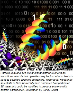
If you can make a single photon, tell it how to spin and tell it where to go, you have a basic element for next-generation computers that work with light instead of wires.
That appears to be possible with atom-thick materials, as demonstrated by several labs. Now, Rice University scientists have developed an understanding of the mechanism by which two-dimensional materials can be manipulated to produce the desired photons.
The Rice lab of materials theorist Boris Yakobson reported this month that by adding pre-arranged imperfections to atom-thick materials like molybdenum disulfide, they become perfectly capable of emitting single photons in either left or right polarization on demand.
The photons come from designer defects in the 2D lattice that add their own peculiar electronic properties to semiconducting materials. In the case of molybdenum disulfide—their best candidate so far—a dash of rhenium in just the right spot makes a configuration of atoms with energy states that sit comfortably inside and are isolated from the material’s natural band gap.
Once in place, the magnetic moments of atoms in the defect can be aligned with a polarized magnet. Exciting them with light brings them to a higher energetic state, but the band gap is large enough that the energy has only one way to go: out, as a coveted single photon.
“Atoms that make up the defect have magnetic moments that can be random, but a magnetic field can bring them to a particular quantum state, either up or down,” Yakobson said. “After that, if you shine light on the defect, it goes from its ground state to an excited state and emits a desirable single photon, with specific polarization. That makes it a bit, which will be useful in quantum information processing.”
“The defect’s optical transition lies in the optical fiber telecommunication band, which is ideal for integration into photonic circuits,” added Rice graduate student and lead author Sunny Gupta.
All of the 2D candidates modeled by Yakobson, Gupta and alumnus Ji-Hui Yang are dichalcogenides, semiconductors that incorporate transition metals and chalcogens. They also modeled tungsten diselenide, zirconium disulfide, boron nitride, tungsten disufide, diamane (2D diamond, which labs are beginning to synthesize) and, for comparison, 3D diamond.
“One of the advantages we argue here relative to 3D materials is that extraction of the photon is much easier, because the material is basically transparent and there is so little thickness,” Yakobson said. “Photons are not so easy to extract from 3D materials, because they may get stopped by internal reflections, or be refracted, or just dissipate in the material. But 2D materials are more open and the photon is produced near the surface, making its extraction for utility easier.”
Where that photon goes, nobody knows just yet. “We know the material can produce a photon of well-defined polarization and energy, and we suspect for good reasons that its direction is also well-defined, yet only probabilistically,” Yakobson said. “But we don’t want to go too far with the theories before somebody tries to make it in the lab.”
Share on:


Testimonial
"The I-Connect007 team is outstanding—kind, responsive, and a true marketing partner. Their design team created fresh, eye-catching ads, and their editorial support polished our content to let our brand shine. Thank you all! "
Sweeney Ng - CEE PCBSuggested Items
ITW EAE Despatch Ovens Now Support ASTM 5423 Testing
10/15/2025 | ITW EAEAs the demand for high-performance electrical insulation materials continues to grow—driven by the rapid expansion of electric vehicles (EVs) and energy storage systems—thermal processing has become a critical step in material development.
Beyond Thermal Conductivity: Exploring Polymer-based TIM Strategies for High-power-density Electronics
10/13/2025 | Padmanabha Shakthivelu and Nico Bruijnis, MacDermid Alpha Electronics SolutionsAs power density and thermal loads continue to increase, effective thermal management becomes increasingly important. Rapid and efficient heat transfer from power semiconductor chip packages is essential for achieving optimal performance and ensuring long-term reliability of temperature-sensitive components. This is particularly crucial in power systems that support advanced applications such as green energy generation, electric vehicles, aerospace, and defense, along with high-speed computing for data centers and artificial intelligence (AI).
Is Glass Finally Coming of Age?
10/13/2025 | Nolan Johnson, I-Connect007Substrates, by definition, form the base of all electronic devices. Whether discussing silicon wafers for semiconductors, glass-and-epoxy materials in printed circuits, or the base of choice for interposers, all these materials function as substrates. While other substrates have come and gone, silicon and FR-4 have remained the de facto standards for the industry.
Creative Materials to Showcase Innovative Functional Inks for Medical Devices at COMPAMED 2025
10/09/2025 | Creative Materials, Inc.Creative Materials, a leading manufacturer of high-performance functional inks and coatings, is pleased to announce its participation in COMPAMED 2025, taking place November 17–20 in Düsseldorf, Germany.
Jiva Leading the Charge Toward Sustainable Innovation
09/30/2025 | Marcy LaRont, PCB007 MagazineEnvironmental sustainability in business—product circularity—is a high priority these days. “Circularity,” the term meant to replace “recycling,” in its simplest definition, describes a full circle life for electronic products and all their elements. The result is re-use or a near-complete reintroduction of the base materials back into the supply chain, leaving very little left for waste. For what cannot be reused productively, the ultimate hope is to have better, less harmful means of disposal and/or materials that can seamlessly and harmlessly decompose and integrate back into the natural environment. That is where Jiva and Soluboard come in.