


 The Marketing Minute: Marketing With Layers
 The Right Approach: Electro-Tek—A Williams Family Legacy, Part 1
 It’s Only Common Sense: If You’re Not Differentiated, You’re Dead


Scientists Design New Material to Harness Power of Light
December 18, 2018 | UMass LowellEstimated reading time: 2 minutes
Scientists have long known that synthetic materials—called metamaterials—can manipulate electromagnetic waves such as visible light to make them behave in ways that cannot be found in nature. That has led to breakthroughs such as super-high resolution imaging. Now, UMass Lowell is part of a research team that is taking the technology of manipulating light in a new direction.
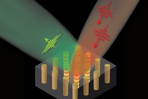
Image Caption: This illustration shows two incoming (red) photons being converted into one reflected (green) photon as result of light interaction with the nanowire structure in the metamaterial. The nanowires are about 100 nanometers apart from center to center, which is about one-fifty-thousandth the diameter of human hair.
The team—which includes collaborators from UMass Lowell, King’s College London, Paris Diderot University and the University of Hartford—has created a new class of metamaterial that can be “tuned” to change the color of light. This technology could someday enable on-chip optical communication in computer processors, leading to smaller, faster, cheaper and more power-efficient computer chips with wider bandwidth and better data storage, among other improvements. On-chip optical communication can also create more efficient fiber-optic telecommunication networks.
“Today’s computer chips use electrons for computing. Electrons are good because they’re tiny,” said Prof. Viktor Podolskiy of the Department of Physics and Applied Physics, who is the project’s principal investigator at UMass Lowell. “However, the frequency of electrons is not fast enough. Light is a combination of tiny particles, called photons, which don’t have mass. As a result, photons could potentially increase the chip’s processing speed.”
By converting electrical signals into pulses of light, on-chip communication will replace obsolete copper wires found on conventional silicon chips, Podolskiy explained. This will enable chip-to-chip optical communication and, ultimately, core-to-core communication on the same chip.
“The end result would be the removal of the communication bottleneck, making parallel computing go so much faster,” he said, adding that the energy of photons determines the color of light. “The vast majority of everyday objects, including mirrors, lenses and optical fibers, can steer or absorb these photons. However, some materials can combine several photons together, resulting in a new photon of higher energy and of different color.”
Podolskiy says enabling the interaction of photons is key to information processing and optical computing. “Unfortunately, this nonlinear process is extremely inefficient and suitable materials for promoting the photon interaction are very rare.”
Podolskiy and the research team have discovered that several materials with poor nonlinear characteristics can be combined together, resulting in a new metamaterial that exhibits desired state-of-the-art nonlinear properties.
“The enhancement comes from the way the metamaterial reshapes the flow of photons,” he said. “The work opens a new direction in controlling the nonlinear response of materials and may find applications in on-chip optical circuits, drastically improving on-chip communications.”
Share on:


Testimonial
"Advertising in PCB007 Magazine has been a great way to showcase our bare board testers to the right audience. The I-Connect007 team makes the process smooth and professional. We’re proud to be featured in such a trusted publication."
Klaus Koziol - atgSuggested Items
Episode 6 of Ultra HDI Podcast Series Explores Copper-filled Microvias in Advanced PCB Design and Fabrication
10/15/2025 | I-Connect007I-Connect007 has released Episode 6 of its acclaimed On the Line with... American Standard Circuits: Ultra High Density Interconnect (UHDI) podcast series. In this episode, “Copper Filling of Vias,” host Nolan Johnson once again welcomes John Johnson, Director of Quality and Advanced Technology at American Standard Circuits, for a deep dive into the pros and cons of copper plating microvias—from both the fabricator’s and designer’s perspectives.
Nolan’s Notes: Tariffs, Technologies, and Optimization
10/01/2025 | Nolan Johnson -- Column: Nolan's NotesLast month, SMT007 Magazine spotlighted India, and boy, did we pick a good time to do so. Tariff and trade news involving India was breaking like a storm surge. The U.S. tariffs shifted India from one of the most favorable trade agreements to the least favorable. Electronics continue to be exempt for the time being, but lest you think that we’re free and clear because we manufacture electronics, steel and aluminum are specifically called out at the 50% tariff levels.
MacDermid Alpha & Graphic PLC Lead UK’s First Horizontal Electroless Copper Installation
09/30/2025 | MacDermid Alpha & Graphic PLCMacDermid Alpha Electronics Solutions, a leading supplier of integrated materials and chemistries to the electronics industry, is proud to support Graphic PLC, a Somacis company, with the installation of the first horizontal electroless copper metallization process in the UK.
Electrodeposited Copper Foils Market to Grow by $11.7 Billion Over 2025-2032
09/18/2025 | Globe NewswireThe global electrodeposited copper foils market is poised for dynamic growth, driven by the rising adoption in advanced electronics and renewable energy storage solutions.
MacDermid Alpha Showcases Advanced Interconnect Solutions at PCIM Asia 2025
09/18/2025 | MacDermid Alpha Electronics SolutionsMacDermid Alpha Electronic Solutions, a global leader in materials for power electronics and semiconductor assembly, will showcase its latest interconnect innovations in electronic interconnect materials at PCIM Asia 2025, held from September 24 to 26 at the Shanghai New International Expo Centre, Booth N5-E30