


 The Marketing Minute: Marketing With Layers
 The Right Approach: Electro-Tek—A Williams Family Legacy, Part 1
 It’s Only Common Sense: If You’re Not Differentiated, You’re Dead


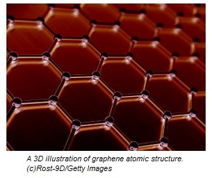
Graphene’s Magic is in the Defects
December 21, 2018 | NYUEstimated reading time: 2 minutes
A team of NYU researchers has solved a longstanding puzzle of how to build ultra-sensitive, ultra-small electrochemical sensors with homogenous and predictable properties by discovering how to engineer graphene structure on an atomic level.
A team of researchers at the New York University Tandon School of Engineering and NYU’s Center for Neural Science has solved a longstanding puzzle of how to build ultra-sensitive, ultra-small electrochemical sensors with homogenous and predictable properties by discovering how to engineer graphene structure on an atomic level.
Finely tuned electrochemical sensors (also referred to as electrodes) that are as small as biological cells are prized for medical diagnostics and environmental monitoring systems. Demand has spurred efforts to develop nanoengineered carbon-based electrodes, which offer unmatched electronic, thermal, and mechanical properties. Yet these efforts have long been stymied by the lack of quantitative principles to guide the precise engineering of the electrode sensitivity to biochemical molecules.
Davood Shahrjerdi, an assistant professor of electrical and computer engineering at NYU Tandon, and Roozbeh Kiani, an assistant professor of neural science and psychology at the Center for Neural Science, have revealed the relationship between various structural defects in graphene and the sensitivity of the electrodes made of it. This discovery opens the door for the precise engineering and industrial-scale production of homogeneous arrays of graphene electrodes.
Graphene is a single, atom-thin sheet of carbon. There is a traditional consensus that structural defects in graphene can generally enhance the sensitivity of electrodes constructed from it. However, a firm understanding of the relationship between various structural defects and the sensitivity has long eluded researchers. This information is particularly vital for tuning the density of different defects in graphene in order to achieve a desired level of sensitivity.
“Until now, achieving a desired sensitivity effect was akin to voodoo or alchemy — oftentimes, we weren’t sure why a certain approach yielded a more or less sensitive electrode,” Shahrjerdi said. “By systematically studying the influence of various types and densities of material defects on the electrode’s sensitivity, we created a physics-based microscopic model that replaces superstition with scientific insight.”
In a surprise finding, the researchers discovered that only one group of defects in graphene’s structure — point defects — significantly impacts electrode sensitivity, which increases linearly with the average density of these defects, within a certain range. “If we optimize these point defects in number and density, we can create an electrode that is up to 20 times more sensitive than conventional electrodes,” Kiani explained.
These findings stand to impact both the fabrication of and applications for graphene-based electrodes. Today’s carbon-based electrodes are calibrated for sensitivity post-fabrication, a time-consuming process that hampers large-scale production, but the researchers’ findings will allow for the precise engineering of the sensitivity during the material synthesis, thereby enabling industrial-scale production of carbon-based electrodes with reliable and reproducible sensitivity.
Currently, carbon-based electrodes are impractical for any application that requires a dense array of sensors: The results are unreliable due to large variations of the electrode-to-electrode sensitivity within the array. These new findings will enable the use of ultra-small carbon-based electrodes with homogeneous and extraordinarily high sensitivities in next-generation neural probes and multiplexed “lab-on-a-chip” platforms for medical diagnostics and drug development, and they may replace optical methods for measuring biological samples including DNA.
Share on:


Testimonial
"In a year when every marketing dollar mattered, I chose to keep I-Connect007 in our 2025 plan. Their commitment to high-quality, insightful content aligns with Koh Young’s values and helps readers navigate a changing industry. "
Brent Fischthal - Koh YoungSuggested Items
Keysight Completes Acquisition of Synopsys’ Optical Solutions Group and Ansys’ PowerArtist
10/17/2025 | Keysight Technologies, Inc.Keysight Technologies, Inc., announced the completion of its acquisitions of the Optical Solutions Group from Synopsys, Inc., and PowerArtist from Ansys, Inc.
New Fil Arzola Class: Designing for the Future, and for Sustainability
10/07/2025 | Andy Shaughnessy, I-Connect007If you have not yet taken a class from Fil Arzola, you are missing out. In late October, Fil will be teaching the class "Building Sustainable Model-Based PCBs," speaking from the design perspective. I had the pleasure of catching this course at last year's IPC APEX EXPO, and I walked away with a lot to think about. I asked Fil to discuss his upcoming course. Registration is open now.
Happy’s Tech Talk #43: Engineering Statistics Training With Free Software
10/06/2025 | Happy Holden -- Column: Happy’s Tech TalkIn over 50 years as a PCB process engineer, the one skill I acquired in college that has been most beneficial is engineering statistics. Basic statistics was part of my engineering fundamentals classes, but I petitioned the dean to let me take the engineering statistics graduate course because I was creating a senior thesis for my honors focus and needed more training on Design of Experiments (DOE).
Looking to Reduce Your Consumables Spend? Visit ROCKA Solutions at SMTA International
09/29/2025 | ROCKA SolutionsROCKA Solutions, a trusted North American manufacturer and distributor of high-quality consumables for the electronics manufacturing industry, is pleased to announce its participation at SMTA International 2025, taking place October 19–23, 2025, at the Donald E. Stephens Convention Center in Rosemont, Illinois. Attendees can connect with the ROCKA team at Booth #2413.
Indium Experts to Present on Thermal Interface Materials at IMAPS Microelectronics Symposium
09/24/2025 | Indium CorporationIndium Corporation experts will deliver technical presentations on thermal interface materials (TIMs) at the International Symposium on Microelectronics, organized by the International Microelectronics Assembly and Packaging Society (IMAPS), to be held from September 29 to October 2 in San Diego, California.