


 The Marketing Minute: Marketing With Layers
 The Right Approach: Electro-Tek—A Williams Family Legacy, Part 1
 It’s Only Common Sense: If You’re Not Differentiated, You’re Dead


Scientists Use Magnetic Defects to Achieve Electromagnetic Wave Breakthrough
December 26, 2018 | Argonne National LaboratoryEstimated reading time: 2 minutes
Surfers spend much of their time watching long waves come onto the shoreline as they attempt to catch one right as it begins to curve and break.
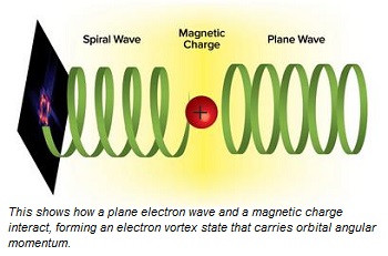
In a similar vein, scientists are working to create twisting helical electromagnetic waves whose curvature allows more accurate imaging of the magnetic properties of different materials at the atomic level and could possibly lead to the development of future devices.
When scientists use electron beams to look at samples of materials, they have the ability to modify many different aspects of the electromagnetic waves that make up the beam. They can make the amplitude of the waves bigger or smaller, or make the waves faster or slower. However, until now there has been no easy way to transform a plane wave — like the long rolling waves out at sea — into a helical wave, like the ones that crash on shore.
In a new study from the U.S. Department of Energy’s (DOE) Argonne National Laboratory, scientists have created small regions of magnetic defects made from nanoscale magnetic islands assembled into a grid. The plane waves interact with these defects, thereby generating helical waves.
“We’re looking for waves with a kind of perfect curl, and in order to generate the curl we need to give them something to crash into, which in our case are magnetic monopoles,” said Argonne materials scientist Charudatta (C.D.) Phatak.
The reason scientists are so interested in helical waves is that they have a property called orbital angular momentum. Knowing the orbital angular momentum of an electron beam allows scientists to investigate the magnetic behavior of materials at an atomic level by determining an atomic property called the magnetic moment.
“If we can see the magnetic moments of the material, we can build a description of the total magnetic properties of the material, and how the material will manifest its electronic and magnetic properties,” Phatak said.
In this way, the refigured electron beam could be useful for studying materials in which spin and magnetization play a crucial role, potentially paving the way towards new forms of electronic devices.
Having access to the information encoded by orbital angular momentum will also allow scientists to better understand the nuances of chiral materials, which have a kind of left- or right-handedness that determines their properties.
The grid of defects can be inserted into any transmission electron microscope to provide a direct way of imaging the sample. “People usually don’t think about modifying the beam profile itself in this way,” Phatak said.
In the next phase of the experiment, Phatak explained that the researchers may seek to replace the grids of magnetic islands with solenoids, or coils of wire that can act as electromagnets. Using solenoids would allow the creation of more precisely tuned magnetic defects. “Right now, because of the arrangement of the magnetic grid, we can only create defects with a cumulative magnetization of two or four, but solenoids would allow us to have a much broader range of magnetization states,” Phatak said.
Share on:


Testimonial
"Advertising in PCB007 Magazine has been a great way to showcase our bare board testers to the right audience. The I-Connect007 team makes the process smooth and professional. We’re proud to be featured in such a trusted publication."
Klaus Koziol - atgSuggested Items
ITW EAE Despatch Ovens Now Support ASTM 5423 Testing
10/15/2025 | ITW EAEAs the demand for high-performance electrical insulation materials continues to grow—driven by the rapid expansion of electric vehicles (EVs) and energy storage systems—thermal processing has become a critical step in material development.
Beyond Thermal Conductivity: Exploring Polymer-based TIM Strategies for High-power-density Electronics
10/13/2025 | Padmanabha Shakthivelu and Nico Bruijnis, MacDermid Alpha Electronics SolutionsAs power density and thermal loads continue to increase, effective thermal management becomes increasingly important. Rapid and efficient heat transfer from power semiconductor chip packages is essential for achieving optimal performance and ensuring long-term reliability of temperature-sensitive components. This is particularly crucial in power systems that support advanced applications such as green energy generation, electric vehicles, aerospace, and defense, along with high-speed computing for data centers and artificial intelligence (AI).
Is Glass Finally Coming of Age?
10/13/2025 | Nolan Johnson, I-Connect007Substrates, by definition, form the base of all electronic devices. Whether discussing silicon wafers for semiconductors, glass-and-epoxy materials in printed circuits, or the base of choice for interposers, all these materials function as substrates. While other substrates have come and gone, silicon and FR-4 have remained the de facto standards for the industry.
Creative Materials to Showcase Innovative Functional Inks for Medical Devices at COMPAMED 2025
10/09/2025 | Creative Materials, Inc.Creative Materials, a leading manufacturer of high-performance functional inks and coatings, is pleased to announce its participation in COMPAMED 2025, taking place November 17–20 in Düsseldorf, Germany.
Jiva Leading the Charge Toward Sustainable Innovation
09/30/2025 | Marcy LaRont, PCB007 MagazineEnvironmental sustainability in business—product circularity—is a high priority these days. “Circularity,” the term meant to replace “recycling,” in its simplest definition, describes a full circle life for electronic products and all their elements. The result is re-use or a near-complete reintroduction of the base materials back into the supply chain, leaving very little left for waste. For what cannot be reused productively, the ultimate hope is to have better, less harmful means of disposal and/or materials that can seamlessly and harmlessly decompose and integrate back into the natural environment. That is where Jiva and Soluboard come in.