


 The Marketing Minute: Marketing With Layers
 The Right Approach: Electro-Tek—A Williams Family Legacy, Part 1
 It’s Only Common Sense: If You’re Not Differentiated, You’re Dead


Better Characterization of Ultra-Thin Materials
December 27, 2018 | DTUEstimated reading time: 3 minutes
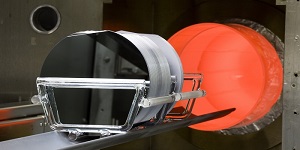
A new optical technology may revolutionize the semiconductor industry and create brand new possibilities within sustainable electronics and data handling. The project is subsidized by Innovation Fund Denmark.
We take it for granted that a new smartphone or tablet is faster than its obsolete predecessor. It has more memory, is thinner, and its touch screen is crystal-clear with a fast response rate. In a few years it may even be flexible, allowing you to roll it up and put it in your pocket.
We expect that renewable energy from solar and wind power will become increasingly efficient and profitable, and that electric cars and trains will play a major role in a future sustainable society and for our environment.
The semiconductor industry is one of the driving forces behind this development. It provides the processing power for handling the astronomical data volumes produced, and delivers efficient components for high-power electronics.
The new Innovation Fund project TRIM has a total budget of EUR 3.7 million (DKK 27 million) and is subsidized by Innovation Fund Denmark with EUR 2.6 million (DKK 19 million).
The aim is to develop optical technology based on terahertz radiation, which can measure the quality of electric and magnetic materials for the semiconductor industry. This ensures high-quality and homogeneous materials.
“Some of the key words for the continued development of a sustainable information society is increased speed, greater storage capacity and higher reliability. All of these require control and quality assurance. Terahertz technology has been the focus of research around the world for many years—now the time has come to bring a huge basic research investment into the real world and prove the value of the technology,” says Peter Uhd Jepsen, Professor, DTU Fotonik, who will be heading the project for the next three years.
The technology offers unique opportunities for completely contactless measurements—a property in high demand by industry, and an essential requirement for the characterization of e.g. 2D materials consisting of one or only a few layers of atoms.
The development of the TRIM technology takes place in close collaboration between DTU and the companies Capres A/S, Topsil GlobalWafers A/S, and NKT Photonics A/S.
The project links the world’s leading competences within terahertz and laser technology, silicon fabrication, and semiconductor materials characterization. It introduces completely new technology and methodology into a conservative and notoriously cautious industry.
“Denmark has a strong position within characterization of materials for the semiconductor industry, but there is still some way to go before we can roll out our laboratory experience to industry. The investment from Innovation Fund Denmark will help us overcome the technological and commercial barriers, which are completely natural, but must be broken down to ensure acceptance of new technologies and methods,” says Peter Uhd Jepsen.
Three of Denmark’s leading companies within semiconductors participate in the project and see great opportunities in getting direct access to world-leading research within this area:
“Capres A/S expects the TRIM project to lead to a significant expansion of the market potential for sales of advanced and fully automated machines to both current and new semiconductor industry customers. For Capres A/S, this will entail that the current unique multi-pin nanoprobe and microprobe-based measuring technique, combined with the new contactless optical measurements, extends the scope and measuring speed within materials characterization, process optimization, and process control,” says Peter Folmer Nielsen, CTO and co-founder, Capres A/S.
“NKT Photonics A/S has achieved great success since its founding by being at the forefront where technology is created. The TRIM project is a prime example of a technology under development with the potential to strengthen Danish high-tech industry as a key supplier to the huge semiconductor industry. The role of NKT Photonics A/S in TRIM is to develop and supply laser systems for the project. The project has extremely high phase noise requirements for the laser systems
Share on:


Testimonial
"Your magazines are a great platform for people to exchange knowledge. Thank you for the work that you do."
Simon Khesin - Schmoll MaschinenSuggested Items
SEMICON West: The Path to a $1 Trillion Future
10/14/2025 | Marcy LaRont, I-Connect007After more than 50 years in San Francisco, SEMICON West moved its 2025 show to Phoenix, which is significant because it highlights the importance of Arizona as a semiconductor and tech hub. Though the show will be back in San Francisco in 2026, the overwhelmingly warm welcome SEMI received from Arizona Governor Katie Hobbs, Phoenix Mayor Kate Gallego, and ASU President Michael Crowe—who has been responsible for ASU repeatedly achieving the U.S. News and World Reports most innovative university ranking—was remarked upon repeatedly. All indications are that SEMICON West may well be back in Phoenix after that 2026 season.
Technica USA Named Exclusive U.S. Distributor for DCT Cleaning Products
10/14/2025 | Technica USATechnica USA is pleased to announce a strategic partnership with DCT USA, LLC, becoming the exclusive master distributor of DCT cleaning products in the United States, effective November 1, 2025.
Is Glass Finally Coming of Age?
10/13/2025 | Nolan Johnson, I-Connect007Substrates, by definition, form the base of all electronic devices. Whether discussing silicon wafers for semiconductors, glass-and-epoxy materials in printed circuits, or the base of choice for interposers, all these materials function as substrates. While other substrates have come and gone, silicon and FR-4 have remained the de facto standards for the industry.
Amplifying Innovation: New Podcast Series Spotlights Electronics Industry Leaders
10/08/2025 | I-Connect007In the debut episode, “Building Reliability: KOKI’s Approach to Solder Joint Challenges,” host Marcy LaRont speaks with Shantanu Joshi, Head of Customer Solutions and Operational Excellence at KOKI Solder America. They explore how advanced materials, such as crack-free fluxes and zero-flux-residue solder pastes, are addressing issues like voiding, heat dissipation, and solder joint reliability in demanding applications, where failure can result in costly repairs or even catastrophic loss.
The Training Connection, LLC Welcomes Industry Veteran Jack Harris to Lead Training Partnerships
10/07/2025 | The Training Connection LLCThe Training Connection, LLC (TTC-LLC), a premier provider of test engineering and development training, is proud to announce that Jack Harris, one of the most recognized names in electronics manufacturing training and technical development, has joined the company as Relationship Lead, Training.