


 The Marketing Minute: Marketing With Layers
 The Right Approach: Electro-Tek—A Williams Family Legacy, Part 1
 It’s Only Common Sense: If You’re Not Differentiated, You’re Dead


Researchers Explore the Prospects for Creating Photonic Integrated Circuits
December 31, 2018 | Lobachevsky UniversityEstimated reading time: 2 minutes
Lobachevsky University scientists' research refutes claims of plasmon amplification on the non-stationary graphene surface, thus providing the groundwork for the theoretical description of electromagnetic phenomena in non-stationary microwaveguides.
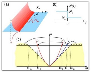
Image Caption: (a) Illustration of a surface plasmon propagating along a graphene sheet at t<0. (b) Time dependence of the graphene carrier density. (c) Dispersion diagram showing the frequency transformation of the initial plasmon when the carrier density decreases from N1 to N2. The lines labeled by 1 and 2 are the dispersion curves for the plasmons at densities N1 and N2, respectively. The shaded region shows the continuous spectrum for bulk waves; the hatched region defines the spectrum of the generated transient radiation. (Image: Lobachevsky University)
The transition from electronic integrated circuits to faster, more energy-efficient and interference-free optical circuits is one of the most important goals in the development of photon technologies. Photonic integrated circuits (PICs) are already used today for transmitting and processing signals in optical networks and communication systems, including, for example, I/O multiplexers of optical signals and microchips with an integrated semiconductor laser, a modulator and a light amplifier. However, today PICs are mostly used in combination with electronic circuits, while purely photonic devices are not yet competitive.
One of the challenges in creating PICs is the complexity of manufacturing various devices (waveguide couplers, power dividers, amplifiers, modulators, lasers and detectors on a single microchip), since they require different materials. The main materials used in existing PICs are semiconductors (indium phosphate, gallium arsenide, silicon), electro-optical crystals (lithium niobate), as well as various types of glass.
In order to increase the speed of PICs in controlling light flux, researchers are searching for new materials with high optical nonlinearity. Among promising materials, one can name, in particular, microwaveguides based on the newly discovered material, graphene (a layer of carbon atoms one atom thick), in which charge carrier concentrations can be effectively controlled using optical pumping or applied bias voltage.
According to Mikhail Bakunov, Head of the UNN General Physics Department, recent theoretical and experimental work shows the possibility of superfast (involving times of several light field periods) carrier concentration changes in graphene, which opens up possibilities for manipulating the amplitude and frequency of light waves (plasmons) directed by the graphene surface.
"The development of physical models for the description of electromagnetic processes in nonstationary graphene is of great practical importance. It causes an increased interest on the part of researchers. One of the results of research in 2018 was the prediction in a number of papers of the possibility to enhance (increase the energy) of plasmons by changing the carrier concentration in graphene, which is certainly attractive for creating new devices," notes Mikhail Bakunov.
Alexei Maslov, Associate Professor at the UNN General Physics Department, continues: "Our study is aimed at developing the physical principles of ultrafast photon control in integrated microchips, in other words, at improving the performance of microcircuits and microchips used in microelectronics and nanoelectronics".
Researchers of the UNN General Physics Department have developed a theory for the conversion of light waves propagating over the surface of graphene (a layer of carbon atoms one atom thick), when the concentration of electrons in graphene changes over time. In contrast to previous research, the interaction of electrons with the light field is precisely taken into account. One of the results of the study was to rule out the previously predicted possibility of amplifying light waves by changing the concentration of electrons. Thus, the work of UNN scientists gives a new look at the dynamics of waves in non-stationary microwaveguides, thereby contributing to the development of PICs.
Share on:


Testimonial
"Our marketing partnership with I-Connect007 is already delivering. Just a day after our press release went live, we received a direct inquiry about our updated products!"
Rachael Temple - AlltematedSuggested Items
ITW EAE Despatch Ovens Now Support ASTM 5423 Testing
10/15/2025 | ITW EAEAs the demand for high-performance electrical insulation materials continues to grow—driven by the rapid expansion of electric vehicles (EVs) and energy storage systems—thermal processing has become a critical step in material development.
Beyond Thermal Conductivity: Exploring Polymer-based TIM Strategies for High-power-density Electronics
10/13/2025 | Padmanabha Shakthivelu and Nico Bruijnis, MacDermid Alpha Electronics SolutionsAs power density and thermal loads continue to increase, effective thermal management becomes increasingly important. Rapid and efficient heat transfer from power semiconductor chip packages is essential for achieving optimal performance and ensuring long-term reliability of temperature-sensitive components. This is particularly crucial in power systems that support advanced applications such as green energy generation, electric vehicles, aerospace, and defense, along with high-speed computing for data centers and artificial intelligence (AI).
Is Glass Finally Coming of Age?
10/13/2025 | Nolan Johnson, I-Connect007Substrates, by definition, form the base of all electronic devices. Whether discussing silicon wafers for semiconductors, glass-and-epoxy materials in printed circuits, or the base of choice for interposers, all these materials function as substrates. While other substrates have come and gone, silicon and FR-4 have remained the de facto standards for the industry.
Creative Materials to Showcase Innovative Functional Inks for Medical Devices at COMPAMED 2025
10/09/2025 | Creative Materials, Inc.Creative Materials, a leading manufacturer of high-performance functional inks and coatings, is pleased to announce its participation in COMPAMED 2025, taking place November 17–20 in Düsseldorf, Germany.
Jiva Leading the Charge Toward Sustainable Innovation
09/30/2025 | Marcy LaRont, PCB007 MagazineEnvironmental sustainability in business—product circularity—is a high priority these days. “Circularity,” the term meant to replace “recycling,” in its simplest definition, describes a full circle life for electronic products and all their elements. The result is re-use or a near-complete reintroduction of the base materials back into the supply chain, leaving very little left for waste. For what cannot be reused productively, the ultimate hope is to have better, less harmful means of disposal and/or materials that can seamlessly and harmlessly decompose and integrate back into the natural environment. That is where Jiva and Soluboard come in.