


 The Marketing Minute: Marketing With Layers
 The Right Approach: Electro-Tek—A Williams Family Legacy, Part 1
 It’s Only Common Sense: If You’re Not Differentiated, You’re Dead


Scientists Move Quantum Optic Networks a Step Closer to Reality
January 3, 2019 | Argonne National LaboratoryEstimated reading time: 3 minutes
Scientists have moved quantum optic networks a step closer to reality. The ability to precisely control the interactions of light and matter at the nanoscale could help such a network transmit larger amounts of data more quickly and securely than an electrical network.
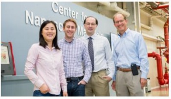
Image Caption: Scientists at Argonne, the University of Chicago and Northwestern University have moved quantum optic networks a step closer to reality with their latest work on semiconducting nanoplatelets that act as tiny light switches. The Argonne team is pictured here. Left to right: Xuedan Ma, Benjamin Diroll, Richard Schaller and Gary Wiederrecht.
A team of researchers at the U.S. Department of Energy’s (DOE) Argonne National Laboratory, the University of Chicago and Northwestern University have successfully surmounted the significant challenges of measuring how nanoplatelets, which consist of two-dimensional layers of cadmium selenide, interact with light in three dimensions. Advances in this area could enhance the operation of quantum optic networks.
“In order to integrate nanoplatelets into, say, photonic devices, we have to understand how they interact with light or how they emit light,” noted Xuedan Ma, nanoscientist at the Center for Nanoscale Materials (CNM), a DOE Office of Science User Facility at Argonne. Ma and six co-authors published their findings in Nano Letters in a paper entitled “Anisotropic photoluminescence from isotropic optical transition dipoles in semiconductor nanoplatelets.”
“The project ultimately targets the unique optical properties of quantum materials and the fact that they emit single photons,” said Gary Wiederrecht, a co-author who also leads the CNM’s nanophotonics and biofunctional structures group. “You have to be able to integrate the quantum emitter with the optical networks.”
Single-photon sources like these are needed for applications in long-distance quantum communications and information processing. These sources, which would serve as signal carriers in quantum optical networks, emit light as single photons (light particles). Single photons are ideal for many quantum information science applications because they travel at light speed and lose little momentum over long distances.
The nanoplatelets form subatomic particle-like entities called excitons when they absorb light. The vertical dimension of the nanoplatelets is where the excitons undergo quantum confinement, a phenomenon that determines their energy levels and parcels electrons into discrete energy levels.
Some of the nanoplatelets for this research, which have remarkably uniform thickness, were synthesized in chemistry professor Dmitri Talapin’s University of Chicago laboratory. Talapin is another co-author of the paper and has a joint appointment with Argonne.
“They have precise atomic-level control of nanoplatelet thickness,” Ma said of Talapin’s research group.
The nanoplatelets are approximately 1.2 nanometers thick (spanning four layers of atoms) and between 10 and 40 nanometers wide. A piece of paper would be thicker than a stack of more than 40,000 nanoplatelets. This makes it harder to measure the material’s interactions with light in three dimensions.
Ma and her colleagues were able to trick the two-dimensional nanoplatelet material into revealing how they interact with light in three dimensions via the special sample preparation and analysis capabilities available at the CNM.
The transition dipole moment is an important three-dimensional parameter operating on semiconductors and organic molecules. “It defines, basically, how the molecule or the semiconductor interacts with external light,” Ma said.
But the vertical component of the transition dipole is difficult to measure in a material as flat as the semiconducting nanoplatelets. The researchers solved that difficulty by using the dry-etching tools of the CNM’s nanofabrication cleanroom to slightly roughen the flat glass slides upon which the nanoplatelets are placed for close examination via laser scanning and microscopy.
“The roughness is not so large that they distort a laser beam, but enough to introduce random distributions of the nanoplatelets,” Ma explained. The random orientations of the nanoplatelets allowed the researchers to assess the three-dimensional dipole properties of the material by special optical methods to create a doughnut-shaped laser beam within a unique optical microscope at the CNM.
The team’s next step is to integrate the nanoplatelet materials with photonic devices for transmitting and processing quantum information. “We’re proceeding in this direction already,” Ma said.
This research was supported by the U.S. Department of Energy’s Office of Science and the National Science Foundation.
Share on:


Testimonial
"In a year when every marketing dollar mattered, I chose to keep I-Connect007 in our 2025 plan. Their commitment to high-quality, insightful content aligns with Koh Young’s values and helps readers navigate a changing industry. "
Brent Fischthal - Koh YoungSuggested Items
ITW EAE Despatch Ovens Now Support ASTM 5423 Testing
10/15/2025 | ITW EAEAs the demand for high-performance electrical insulation materials continues to grow—driven by the rapid expansion of electric vehicles (EVs) and energy storage systems—thermal processing has become a critical step in material development.
Beyond Thermal Conductivity: Exploring Polymer-based TIM Strategies for High-power-density Electronics
10/13/2025 | Padmanabha Shakthivelu and Nico Bruijnis, MacDermid Alpha Electronics SolutionsAs power density and thermal loads continue to increase, effective thermal management becomes increasingly important. Rapid and efficient heat transfer from power semiconductor chip packages is essential for achieving optimal performance and ensuring long-term reliability of temperature-sensitive components. This is particularly crucial in power systems that support advanced applications such as green energy generation, electric vehicles, aerospace, and defense, along with high-speed computing for data centers and artificial intelligence (AI).
Is Glass Finally Coming of Age?
10/13/2025 | Nolan Johnson, I-Connect007Substrates, by definition, form the base of all electronic devices. Whether discussing silicon wafers for semiconductors, glass-and-epoxy materials in printed circuits, or the base of choice for interposers, all these materials function as substrates. While other substrates have come and gone, silicon and FR-4 have remained the de facto standards for the industry.
Creative Materials to Showcase Innovative Functional Inks for Medical Devices at COMPAMED 2025
10/09/2025 | Creative Materials, Inc.Creative Materials, a leading manufacturer of high-performance functional inks and coatings, is pleased to announce its participation in COMPAMED 2025, taking place November 17–20 in Düsseldorf, Germany.
Jiva Leading the Charge Toward Sustainable Innovation
09/30/2025 | Marcy LaRont, PCB007 MagazineEnvironmental sustainability in business—product circularity—is a high priority these days. “Circularity,” the term meant to replace “recycling,” in its simplest definition, describes a full circle life for electronic products and all their elements. The result is re-use or a near-complete reintroduction of the base materials back into the supply chain, leaving very little left for waste. For what cannot be reused productively, the ultimate hope is to have better, less harmful means of disposal and/or materials that can seamlessly and harmlessly decompose and integrate back into the natural environment. That is where Jiva and Soluboard come in.