


 The Marketing Minute: Marketing With Layers
 The Right Approach: Electro-Tek—A Williams Family Legacy, Part 1
 It’s Only Common Sense: If You’re Not Differentiated, You’re Dead


Excitons Pave the Way to More Efficient Electronics
January 4, 2019 | EPFLEstimated reading time: 2 minutes
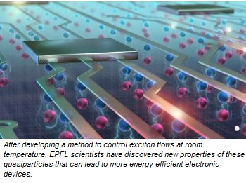
They were the first to control exciton flows at room temperature. And now, the team of scientists from EPFL’s Laboratory of Nanoscale Electronics and Structures (LANES) has taken their technology one step further. They have found a way to control some of the properties of excitons and change the polarization of the light they generate. This can lead to a new generation of electronic devices with transistors that undergo less energy loss and heat dissipation. The scientists’ discovery forms part of a new field of research called valleytronics and has just been published in Nature Photonics.
Excitons are created when an electron absorbs light and moves into a higher energy level, or “energy band” as they are called in solid quantum physics. This excited electron leaves behind an “electron hole” in its previous energy band. And because the electron has a negative charge and the hole a positive charge, the two are bound together by an electrostatic force called a Coulomb force. It’s this electron-electron hole pair that is referred to as an exciton.
Unprecedented Quantum Properties
Excitons exist only in semiconducting and insulating materials. Their extraordinary properties can be easiliy accessed in 2D materials, which are materials whose basic structure is just a few atoms thick. The most common examples of such materials are carbon and molybdenite.
When such 2D materials are combined, they often exhibit quantum properties that neither material possesses on its own. The EPFL scientists thus combined tungsten diselenide (WSe2) with molybdenum diselenide (MoSe2) to reveal new properties with an array of possible high-tech applications. By using a laser to generate light beams with circular polarization, and slightly shifting the positions of the two 2D materials so as to create a moiré pattern, they were able to use excitons to change and regulate the polarization, wavelength and intensity of light.
From One Valley to the Next
The scientists achieved this by manipulating one of the excitons’ properties: their “valley,” which is related to the extremes of energies of the electron and the hole . These valleys – which are where the name valleytronics comes from – can be leveraged to code and process information at a nanoscopic level.
“Linking several devices that incorporate this technology would give us a new way to process data,” says Andras Kis, who heads LANES. “By changing the polarization of light in a given device, we can then select a specific valley in a second device that’s connected to it. That’s similar to switching from 0 to 1 or 1 to 0, which is the fundamental binary logic used in computing.”
Share on:


Testimonial
"Advertising in PCB007 Magazine has been a great way to showcase our bare board testers to the right audience. The I-Connect007 team makes the process smooth and professional. We’re proud to be featured in such a trusted publication."
Klaus Koziol - atgSuggested Items
ITW EAE Despatch Ovens Now Support ASTM 5423 Testing
10/15/2025 | ITW EAEAs the demand for high-performance electrical insulation materials continues to grow—driven by the rapid expansion of electric vehicles (EVs) and energy storage systems—thermal processing has become a critical step in material development.
Beyond Thermal Conductivity: Exploring Polymer-based TIM Strategies for High-power-density Electronics
10/13/2025 | Padmanabha Shakthivelu and Nico Bruijnis, MacDermid Alpha Electronics SolutionsAs power density and thermal loads continue to increase, effective thermal management becomes increasingly important. Rapid and efficient heat transfer from power semiconductor chip packages is essential for achieving optimal performance and ensuring long-term reliability of temperature-sensitive components. This is particularly crucial in power systems that support advanced applications such as green energy generation, electric vehicles, aerospace, and defense, along with high-speed computing for data centers and artificial intelligence (AI).
Is Glass Finally Coming of Age?
10/13/2025 | Nolan Johnson, I-Connect007Substrates, by definition, form the base of all electronic devices. Whether discussing silicon wafers for semiconductors, glass-and-epoxy materials in printed circuits, or the base of choice for interposers, all these materials function as substrates. While other substrates have come and gone, silicon and FR-4 have remained the de facto standards for the industry.
Creative Materials to Showcase Innovative Functional Inks for Medical Devices at COMPAMED 2025
10/09/2025 | Creative Materials, Inc.Creative Materials, a leading manufacturer of high-performance functional inks and coatings, is pleased to announce its participation in COMPAMED 2025, taking place November 17–20 in Düsseldorf, Germany.
Jiva Leading the Charge Toward Sustainable Innovation
09/30/2025 | Marcy LaRont, PCB007 MagazineEnvironmental sustainability in business—product circularity—is a high priority these days. “Circularity,” the term meant to replace “recycling,” in its simplest definition, describes a full circle life for electronic products and all their elements. The result is re-use or a near-complete reintroduction of the base materials back into the supply chain, leaving very little left for waste. For what cannot be reused productively, the ultimate hope is to have better, less harmful means of disposal and/or materials that can seamlessly and harmlessly decompose and integrate back into the natural environment. That is where Jiva and Soluboard come in.