


 The Marketing Minute: Marketing With Layers
 The Right Approach: Electro-Tek—A Williams Family Legacy, Part 1
 It’s Only Common Sense: If You’re Not Differentiated, You’re Dead


Unlocking New Paths Toward High-Temperature Superconductors
January 4, 2019 | Berkeley LabEstimated reading time: 5 minutes
In the 1980s, the discovery of high-temperature superconductors known as cuprates upended a widely held theory that superconductor materials carry electrical current without resistance only at very low temperatures of around 30 Kelvin (or minus 406 degrees Fahrenheit). For decades since, researchers have been mystified by the ability of some cuprates to superconduct at temperatures of more than 100 Kelvin (minus 280 degrees Fahrenheit).
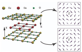
Image Caption: With the spin resolution enabled by SARPES, Berkeley Lab researchers revealed magnetic properties of Bi-2212 that have gone unnoticed in previous studies. (Credit: Kenneth Gotlieb, Chiu-Yun Lin, et al./Berkeley Lab)
Now, researchers at the U.S. Department of Energy’s Lawrence Berkeley National Laboratory (Berkeley Lab) have unveiled a clue into the cuprates’ unusual properties – and the answer lies within an unexpected source: the electron spin.
Adding Electron Spin to the Equation
Every electron is like a tiny magnet that points in a certain direction. And electrons within most superconductor materials seem to follow their own inner compass. Rather than pointing in the same direction, their electron spins haphazardly point every which way – some up, some down, others left or right.
When scientists are developing new kinds of materials, they usually look at the materials’ electron spin, or the direction in which the electrons are pointing. But when it comes to making superconductors, condensed matter physicists haven’t traditionally focused on spin, because the conventionally held view was that all of the properties that make these materials unique were shaped only by the way in which two electrons interact with each other through what’s known as “electron correlation.”
But when a research team led by Alessandra Lanzara, a faculty scientist in Berkeley Lab’s Materials Sciences Division and a Charles Kittel Professor of Physics at UC Berkeley, used a unique detector to measure samples of an exotic cuprate superconductor, Bi-2212 (bismuth strontium calcium copper oxide), with a powerful technique called SARPES (spin- and angle-resolved photoemission spectroscopy), they uncovered something that defied everything they had ever known about superconductors: a distinct pattern of electron spins within the material.
“In other words, we discovered that there was a well-defined direction in which each electron was pointing given its momentum, a property also known as spin-momentum locking,” said Lanzara. “Finding it in high-temperature superconductors was a big surprise.”
A New Map for High-Temperature Superconductors
In the world of superconductors, “high temperature” means that the material can conduct electricity without resistance at temperatures higher than expected but still in extremely cold temperatures far below zero degrees Fahrenheit. That’s because superconductors need to be extraordinarily cold to carry electricity without any resistance. At those low temperatures, electrons are able to move in sync with each other and not get knocked by jiggling atoms, causing electrical resistance.
And within this special class of high-temperature superconductor materials, cuprates are some of the best performers, leading some researchers to believe that they have potential use as a new material for building super-efficient electrical wires that can carry power without any loss of electron momentum, said co-lead author Kenneth Gotlieb, who was a Ph.D. student in Lanzara’s lab at the time of the discovery. Understanding what makes some exotic cuprate superconductors such as Bi-2212 work at temperatures as high as 133 Kelvin (about -220 degrees Fahrenheit) could make it easier to realize a practical device.
Among the very exotic materials that condensed matter physicists study, there are two kinds of electron interactions that give rise to novel properties for new materials, including superconductors, said Gotlieb. Scientists who have been studying cuprate superconductors have focused on just one of those interactions: electron correlation.
The other kind of electron interaction found in exotic materials is “spin-orbit coupling” – the way in which the electron’s magnetic moment interacts with atoms in the material.
Spin-orbit coupling was often neglected in the studies of cuprate superconductors, because many assumed that this kind of electron interaction would be weak when compared to electron correlation, said co-lead author Chiu-Yun Lin, a researcher in the Lab’s Materials Sciences Division and a Ph.D. student in the Department of Physics at UC Berkeley. So when they found the unusual spin pattern, Lin said that although they were pleasantly surprised by this initial finding, they still weren’t sure whether it was a “true” intrinsic property of the Bi-2212 material, or an external effect caused by the way the laser light interacted with the material in the experiment.
Shining a Light on Electron Spin with SARPES
Over the course of nearly three years, Gotlieb and Lin used the SARPES detector to thoroughly map out the spin pattern at Lanzara’s lab. When they needed higher photon energies to excite a wider range of electrons within a sample, the researchers moved the detector next door to Berkeley Lab’s synchrotron, the Advanced Light Source (ALS), a U.S. DOE Office of Science User Facility that specializes in lower energy, “soft” X-ray light for studying the properties of materials.
The SARPES detector was developed by Lanzara, along with co-authors Zahid Hussain, the former ALS Division Deputy, and Chris Jozwiak, an ALS staff scientist. The detector allowed the scientists to probe key electronic properties of the electrons such as valence band structure.
After tens of experiments at the ALS, where the team of researchers connected the SARPES detector to Beamline 10.0.1 so they could access this powerful light to explore the spin of the electrons moving with much higher momentum through the superconductor than those they could access in the lab, they found that Bi-2212’s distinct spin pattern – called “nonzero spin – was a true result, inspiring them to ask even more questions. “There remains many unsolved questions in the field of high-temperature superconductivity,” said Lin. “Our work provides new knowledge to better understand the cuprate superconductors, which can be a building block to resolve these questions.”
Lanzara added that their discovery couldn’t have happened without the collaborative “team science” of Berkeley Lab, a DOE national lab with historic ties to nearby UC Berkeley. “This work is a typical example of where science can go when people with expertise across the scientific disciplines come together, and how new instrumentation can push the boundaries of science,” she said.
Share on:


Testimonial
"Our marketing partnership with I-Connect007 is already delivering. Just a day after our press release went live, we received a direct inquiry about our updated products!"
Rachael Temple - AlltematedSuggested Items
Episode 6 of Ultra HDI Podcast Series Explores Copper-filled Microvias in Advanced PCB Design and Fabrication
10/15/2025 | I-Connect007I-Connect007 has released Episode 6 of its acclaimed On the Line with... American Standard Circuits: Ultra High Density Interconnect (UHDI) podcast series. In this episode, “Copper Filling of Vias,” host Nolan Johnson once again welcomes John Johnson, Director of Quality and Advanced Technology at American Standard Circuits, for a deep dive into the pros and cons of copper plating microvias—from both the fabricator’s and designer’s perspectives.
Nolan’s Notes: Tariffs, Technologies, and Optimization
10/01/2025 | Nolan Johnson -- Column: Nolan's NotesLast month, SMT007 Magazine spotlighted India, and boy, did we pick a good time to do so. Tariff and trade news involving India was breaking like a storm surge. The U.S. tariffs shifted India from one of the most favorable trade agreements to the least favorable. Electronics continue to be exempt for the time being, but lest you think that we’re free and clear because we manufacture electronics, steel and aluminum are specifically called out at the 50% tariff levels.
MacDermid Alpha & Graphic PLC Lead UK’s First Horizontal Electroless Copper Installation
09/30/2025 | MacDermid Alpha & Graphic PLCMacDermid Alpha Electronics Solutions, a leading supplier of integrated materials and chemistries to the electronics industry, is proud to support Graphic PLC, a Somacis company, with the installation of the first horizontal electroless copper metallization process in the UK.
Electrodeposited Copper Foils Market to Grow by $11.7 Billion Over 2025-2032
09/18/2025 | Globe NewswireThe global electrodeposited copper foils market is poised for dynamic growth, driven by the rising adoption in advanced electronics and renewable energy storage solutions.
MacDermid Alpha Showcases Advanced Interconnect Solutions at PCIM Asia 2025
09/18/2025 | MacDermid Alpha Electronics SolutionsMacDermid Alpha Electronic Solutions, a global leader in materials for power electronics and semiconductor assembly, will showcase its latest interconnect innovations in electronic interconnect materials at PCIM Asia 2025, held from September 24 to 26 at the Shanghai New International Expo Centre, Booth N5-E30