


 The Marketing Minute: Marketing With Layers
 The Right Approach: Electro-Tek—A Williams Family Legacy, Part 1
 It’s Only Common Sense: If You’re Not Differentiated, You’re Dead


Powerful X-Ray Beams Unlock Secrets of Nanoscale Crystal Formation
January 7, 2019 | Georgia Institute of TechnologyEstimated reading time: 4 minutes
High-energy X-ray beams and a clever experimental setup allowed researchers to watch a high-pressure, high-temperature chemical reaction to determine for the first time what controls formation of two different nanoscale crystalline structures in the metal cobalt. The technique allowed continuous study of cobalt nanoparticles as they grew from clusters including tens of atoms to crystals as large as five nanometers.
The research provides the proof-of-principle for a new technique to study crystal formation in real-time, with potential applications for other materials, including alloys and oxides. Data from the study produced "nanometric phase diagrams" showing the conditions that control the structure of cobalt nanocrystals as they form.
The research, reported November 13 in the Journal of the American Chemical Society, was sponsored by the National Science Foundation, and used U.S. Department of Energy-supported synchrotron X-ray beam lines at Brookhaven National Laboratory and Argonne National Laboratory.
"We found that we could indeed control formation of the two different crystalline structures, and that the tuning factor was the pH of the solution," said Hailong Chen, an assistant professor in the George W. Woodruff School of Mechanical Engineering at the Georgia Institute of Technology. "Tuning the crystalline structure allowed us to control the functionality and properties of these materials. We believe this methodology could also be applied to alloys and oxides."
In bulk cobalt, crystal formation favors the hexagonal close-pack (HCP) structure because it minimizes energy to create a stable structure. At the nanoscale, however, cobalt also forms the face-centered cubic (FCC) phase, which has a higher energy. That can be stable because the high surface energy of small nanoclusters affects the total crystalline energy, Chen said.
"When the clusters are small, we have more tuning effects, which is controlled by the surface energy of the OH minus group or other ligands," he added. "We can tune the concentration of the OH minus group in the solution so we can tune the surface energy and therefore the overall energy of the cluster."
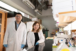
Working with researchers from the two national laboratories and the Department of Materials Science at the University of Maryland, Chen and graduate research assistant Xuetian Ma examined the polymorphic structures using theoretical, experimental and computational modeling techniques.
Experimentally, the researchers reduced cobalt hydroxide in a solution of ethylene glycol, using potassium hydroxide to vary the pH of the solution. The reaction takes place under high pressure - about 1,800 pounds per square inch - and at more than 200 degrees Celsius.
In the laboratory, the researchers use a heavy steel containment vessel that allowed them to analyze only the reaction results. To follow how the reaction took place, they needed to observe it in real time, which required development of a containment vessel small enough to allow for X-ray transmission while handling the high pressure and high temperature at the same time.
The result was a reaction vessel made of a high-strength quartz tube about a millimeter in diameter and about two inches long. After the cobalt hydroxide solution was added, the tube was spun to both facilitate the chemical reaction and average the X-ray signal. A small heater applied the necessary thermal energy and a thermocouple measured the temperature.
Ma and Chen used the setup during four separate trips to beam lines at the National Synchrotron Light Source II at Brookhaven, and the Advanced Photon Source at Argonne National Laboratory. X-rays passing through the reaction chamber to a two-dimensional detector provided continuous monitoring of the chemical reaction, which took about two hours to complete.
"When they started forming a detectable spectrum we captured the X-ray diffraction spectrum and continued to observe it until the crystal cobalt formed," Ma explained. "We were able to observe step-by-step what was happening from initial nucleation to the end of the reaction."
Data obtained by varying the pH of the reaction produced a nanometric phase diagram showing where different combinations produced the two structures.
The X-ray diffraction results confirmed the theoretical predictions and computational modeling done by Yifei Mo, an assistant professor in the A. James Clark School of Engineering at the University of Maryland. Mo and colleagues Adelaide Nolan and Shuo Zhang used density functional theory to describe how the crystal would nucleate under differing conditions.
The success with cobalt suggests the methodology could be used to produce nanometric phase diagrams for other materials, including more complex alloys and oxides, Chen said.
"Our goal was to build a model and a systematic understanding about the formation of crystalline materials at the nanoscale," he said. "Until now, researchers had been relying on empirical design to control growth of the materials. Now we can offer a theoretical model that would allow systematic prediction of what kinds of properties are possible under different conditions."
As a next step, the Georgia Tech researchers plan to study alloys, to further improve the theoretical model and experimental approach.
Share on:


Testimonial
"Our marketing partnership with I-Connect007 is already delivering. Just a day after our press release went live, we received a direct inquiry about our updated products!"
Rachael Temple - AlltematedSuggested Items
ITW EAE Despatch Ovens Now Support ASTM 5423 Testing
10/15/2025 | ITW EAEAs the demand for high-performance electrical insulation materials continues to grow—driven by the rapid expansion of electric vehicles (EVs) and energy storage systems—thermal processing has become a critical step in material development.
Beyond Thermal Conductivity: Exploring Polymer-based TIM Strategies for High-power-density Electronics
10/13/2025 | Padmanabha Shakthivelu and Nico Bruijnis, MacDermid Alpha Electronics SolutionsAs power density and thermal loads continue to increase, effective thermal management becomes increasingly important. Rapid and efficient heat transfer from power semiconductor chip packages is essential for achieving optimal performance and ensuring long-term reliability of temperature-sensitive components. This is particularly crucial in power systems that support advanced applications such as green energy generation, electric vehicles, aerospace, and defense, along with high-speed computing for data centers and artificial intelligence (AI).
Is Glass Finally Coming of Age?
10/13/2025 | Nolan Johnson, I-Connect007Substrates, by definition, form the base of all electronic devices. Whether discussing silicon wafers for semiconductors, glass-and-epoxy materials in printed circuits, or the base of choice for interposers, all these materials function as substrates. While other substrates have come and gone, silicon and FR-4 have remained the de facto standards for the industry.
Creative Materials to Showcase Innovative Functional Inks for Medical Devices at COMPAMED 2025
10/09/2025 | Creative Materials, Inc.Creative Materials, a leading manufacturer of high-performance functional inks and coatings, is pleased to announce its participation in COMPAMED 2025, taking place November 17–20 in Düsseldorf, Germany.
Jiva Leading the Charge Toward Sustainable Innovation
09/30/2025 | Marcy LaRont, PCB007 MagazineEnvironmental sustainability in business—product circularity—is a high priority these days. “Circularity,” the term meant to replace “recycling,” in its simplest definition, describes a full circle life for electronic products and all their elements. The result is re-use or a near-complete reintroduction of the base materials back into the supply chain, leaving very little left for waste. For what cannot be reused productively, the ultimate hope is to have better, less harmful means of disposal and/or materials that can seamlessly and harmlessly decompose and integrate back into the natural environment. That is where Jiva and Soluboard come in.