


 The Marketing Minute: AI Is Watching Your Marketing Habits
 Trouble in Your Tank: The Role of Organic Solderability Preservatives in Advanced Packaging
 It’s Only Common Sense: Lighten Up!


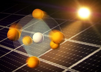
New research could lead to the design of new materials to help improve the performance of perovskite solar cells (PSCs). Perovskite solar cells are an emerging photovoltaic technology that has seen a remarkable rise in power conversion efficiency to above 20%.
However, PSC performance is affected as the perovskite material contains ion defects that can move around over the course of a working day. As these defects move, they affect the internal electric environment within the cell.
The Perovskite material is responsible for absorbing light to create electronic charge, and also for helping to extract the charge into an external circuit before it is lost to a process called ‘recombination.’
The majority of detrimental recombination can occur in different locations within the solar cell. In some designs it occurs predominantly within the perovskite, while in others it happens at the edges of the perovskite where it contacts the adjacent materials known as transport layers.
Researchers from the Universities of Portsmouth, Southampton and Bath have now developed a way to adjust the properties of the transport layers to encourage the ionic defects within the perovskite to move in such a way that they suppress recombination and lead to more efficient charge extraction—increasing the proportion of the light energy falling on the surface of the cell that can ultimately be used.
Dr Jamie Foster from the University of Portsmouth, who was involved in the study, said: “Careful cell design can manipulate the ionic defects to move to regions where they enhance the extraction of electronic charge, thereby increasing the useful power that a cell can deliver.”
The study, published in Energy and Environmental Science, showed that the performance of PSCs are strongly dependent on the permittivity (the measure of a material’s ability to store an electric field) and the effective doping density of the transport layers.
Dr Foster said: “Understanding how and which transport layer properties affect cell performance is vital for informing the design of cell architectures in order to obtain the most power while minimising degradation.
“We found that ion movement plays a significant role in the steady-state device performance, through the resulting accumulation of ionic charge and band bending in narrow layers adjacent to the interfaces between the perovskite and the transport layers. The distribution of the electric potential is key in determining the transient and steady-state behaviour of a cell.
“Further to this, we suggest that the doping density and/or permittivities of each transport layer may be tuned to reduce losses due to interfacial recombination. Once this and the rate limiting charge carrier has been identified, our work provides a systematic tool to tune transport layer properties to enhance performance.”
The researchers also suggest that PSCs made using transport layers with low permittivity and doping are more stable, than those with high permittivity and doping. This is because such cells show reduced ion vacancy accumulation within the perovskite layers, which has been linked to chemical degradation at the edges of the perovskite layer.


