


 The Marketing Minute: Marketing With Layers
 The Right Approach: Electro-Tek—A Williams Family Legacy, Part 1
 It’s Only Common Sense: If You’re Not Differentiated, You’re Dead


Researchers Catalog Defects That Give 2-D Materials Amazing Properties
January 16, 2019 | MITEstimated reading time: 4 minutes
Amid the frenzy of worldwide research on atomically thin materials like graphene, there is one area that has eluded any systematic analysis — even though this information could be crucial to a host of potential applications, including desalination, DNA sequencing, and devices for quantum communications and computation systems.
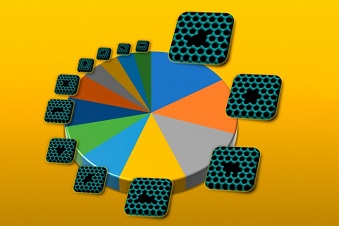
Image Caption: This illustration shows the 12 different forms that six-atom vacancy defects in graphene can have, as determined by the researchers. The pie chart shows the relative abundances that are predicted for each of these different forms. Image: Ananth Govind Rajan
That missing information has to do with the kinds of minuscule defects, or “holes,” that form in these 2-D sheets when some atoms are missing from the material’s crystal lattice.
Now that problem has been solved by researchers at MIT, who have produced a catalog of the exact sizes and shapes of holes that would most likely be observed (as opposed to the many more that are theoretically possible) when a given number of atoms is removed from the atomic lattice. The results are described in the journal Nature Materials in a paper by graduate student Ananth Govind Rajan, professors of chemical engineering Daniel Blankschtein and Michael Strano, and four others at MIT, Lockheed Martin Space, and Oxford University.
“It’s been a longstanding problem in the graphene field, what we call the isomer cataloging problem for nanopores,” Strano says. For those who want to use graphene or similar two-dimensional, sheet-like materials for applications including chemical separation or filtration, he says, “we just need to understand the kinds of atomic defects that can occur,” compared to the vastly larger number that are never seen.
For example, Blankschtein points out, by removing just eight contiguous carbon atoms from the hexagonal chicken-wire-like array of atoms in graphene, there are 66 different possible shapes that the resulting hole could have. When the number of atoms removed increases to 12, the number of possible shapes jumps to 3,226, and with 30 atoms removed, there are 400 billion possibilities — a number far beyond any reasonable possibility of simulation and analysis. Yet only a handful of these shapes are actually found in experiments, so the ability to predict which ones really occur could be of great use to researchers.
Describing the lack of information about which kinds of holes actually can form, Strano says, “What that did, practically speaking, is it made a disconnect between what you could simulate with a computer and what you could actually measure in the lab.” This new catalog of the shapes that are actually possible will make the search for materials for specific uses much more manageable, he says.
The ability to do the analysis relied on a number of tools that simply weren’t available previously. “You could not have solved this problem 10 years ago,” Strano says. But now, with the use of tools including chemical graph theory, accurate electronic-structure calculations, and high-resolution scanning transmission electron microscopy, the researchers have captured images of the defects showing the exact positions of the individual atoms.
The team calls these holes in the lattice “antimolecules” and describes them in terms of the shape that would be formed by the atoms that have been removed. This approach provides, for the first time, a simple and coherent framework for describing the whole set of these complex shapes. Previously, “if you were talking about these pores in the material, there was no way to identify” the specific kind of hole involved, Govind Rajan says. “Once people start creating these pores more often, it would be good to have a naming convention” to identify them, he adds.
This new catalog could help to open up a variety of potential applications. “Defects are both good and bad,” Strano explains. “Sometimes you want to prevent them,” because they weaken the material, but “other times you want to create them and control their sizes and shapes,” for example for filtration, chemical processing, or DNA sequencing, where only certain specific molecules can pass through these holes. Another application might be quantum computing or communications devices where holes of a specific size and shape are tuned to emit photons of light of specific colors and energy levels.
In addition to their impact on a material’s mechanical properties, holes affect electronic, magnetic, and optical characteristics as well, Govind Rajan says.
“We think that this work will constitute a valuable tool” for research on defects in 2-D materials, Strano predicts, because it will allow researchers to home in on promising types of defects instead of having to sort through countless theoretically possible shapes “that you don’t care about at all, because they are so improbable they’ll never form.”
This work “addresses an important problem in 2-D nanoscale systems,” says Alex Zettl, a professor of materials science at the University of California at Berkeley, who was not involved in this research. “Since the defect isomer possibilities become rapidly intractable with growing atom vacancy number, a brute-force attack is fruitless. This new cataloging and probabilistic ranking approach is elegant, relevant, and predictive.”
He says that this work provides “a solid theoretical foundation,” and since engineering of 2-D materials is becoming a reality, this system “is sure to become accepted and widely adopted.”
The research team included Kevin Silmore at MIT, Jacob Swett at Lockheed Martin Space in Palo Alto, California, and Alex Robertson and Jamie Warner at Oxford University. The work was supported by the Army Research Office via the Institute for Soldier Nanotechnologies at MIT, the U.S. Department of Energy, and the National Science Foundation.
Share on:


Testimonial
"In a year when every marketing dollar mattered, I chose to keep I-Connect007 in our 2025 plan. Their commitment to high-quality, insightful content aligns with Koh Young’s values and helps readers navigate a changing industry. "
Brent Fischthal - Koh YoungSuggested Items
ITW EAE Despatch Ovens Now Support ASTM 5423 Testing
10/15/2025 | ITW EAEAs the demand for high-performance electrical insulation materials continues to grow—driven by the rapid expansion of electric vehicles (EVs) and energy storage systems—thermal processing has become a critical step in material development.
Beyond Thermal Conductivity: Exploring Polymer-based TIM Strategies for High-power-density Electronics
10/13/2025 | Padmanabha Shakthivelu and Nico Bruijnis, MacDermid Alpha Electronics SolutionsAs power density and thermal loads continue to increase, effective thermal management becomes increasingly important. Rapid and efficient heat transfer from power semiconductor chip packages is essential for achieving optimal performance and ensuring long-term reliability of temperature-sensitive components. This is particularly crucial in power systems that support advanced applications such as green energy generation, electric vehicles, aerospace, and defense, along with high-speed computing for data centers and artificial intelligence (AI).
Is Glass Finally Coming of Age?
10/13/2025 | Nolan Johnson, I-Connect007Substrates, by definition, form the base of all electronic devices. Whether discussing silicon wafers for semiconductors, glass-and-epoxy materials in printed circuits, or the base of choice for interposers, all these materials function as substrates. While other substrates have come and gone, silicon and FR-4 have remained the de facto standards for the industry.
Creative Materials to Showcase Innovative Functional Inks for Medical Devices at COMPAMED 2025
10/09/2025 | Creative Materials, Inc.Creative Materials, a leading manufacturer of high-performance functional inks and coatings, is pleased to announce its participation in COMPAMED 2025, taking place November 17–20 in Düsseldorf, Germany.
Jiva Leading the Charge Toward Sustainable Innovation
09/30/2025 | Marcy LaRont, PCB007 MagazineEnvironmental sustainability in business—product circularity—is a high priority these days. “Circularity,” the term meant to replace “recycling,” in its simplest definition, describes a full circle life for electronic products and all their elements. The result is re-use or a near-complete reintroduction of the base materials back into the supply chain, leaving very little left for waste. For what cannot be reused productively, the ultimate hope is to have better, less harmful means of disposal and/or materials that can seamlessly and harmlessly decompose and integrate back into the natural environment. That is where Jiva and Soluboard come in.