


 The Marketing Minute: Marketing With Layers
 The Right Approach: Electro-Tek—A Williams Family Legacy, Part 1
 It’s Only Common Sense: If You’re Not Differentiated, You’re Dead


Brilliant Glow of Paint-On Semiconductors Comes from Ornate Quantum Physics
January 16, 2019 | Georgia TechEstimated reading time: 5 minutes
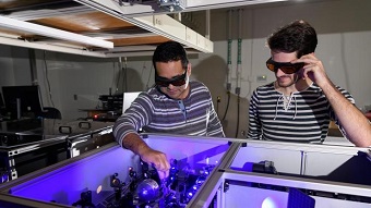
LED lights and monitors, and quality solar panels were born of a revolution in semiconductors that efficiently convert energy to light or vice versa. Now, next-generation semiconducting materials are on the horizon, and in a new study, researchers have uncovered eccentric physics behind their potential to transform lighting technology and photovoltaics yet again.
Comparing the quantum properties of these emerging so-called hybrid semiconductors with those of their established predecessors is about like comparing the Bolshoi Ballet to jumping jacks. Twirling troupes of quantum particles undulate through the emerging materials, creating, with ease, highly desirable optoelectronic (light-electronic) properties, according to a team of physical chemists led by researchers at the Georgia Institute of Technology.
These same properties are impractical to achieve in established semiconductors.
The particles moving through these new materials also engage the material itself in the quantum action, akin to dancers enticing the floor to dance with them. The researchers were able to measure patterns in the material caused by the dancing and relate them to the emerging material’s quantum properties and to energy introduced into the material.
These insights could help engineers work productively with the new class of semiconductors.
Unusually Flexible Semiconductors
The emerging material’s ability to house diverse, eccentric quantum particle movements, analogous to the dancers, is directly related to its unusual flexibility on a molecular level, analogous to the dancefloor that joins in the dances. By contrast, established semiconductors have rigid, straight-laced molecular structures that leave the dancing to quantum particles.
The class of hybrid semiconductors the researchers examined is called halide organic-inorganic perovskite (HOIP), which will be explained in more detail at bottom along with the “hybrid” semiconductor designation, which combines a crystal lattice -- common in semiconductors -- with a layer of innovatively flexing material.
Beyond their promise of unique radiance and energy-efficiency, HOIPs are easy to produce and apply.
Paint Them On
“One compelling advantage is that HOIPs are made using low temperatures and processed in solution,” said Carlos Silva, a professor in Georgia Tech’s School of Chemistry and Biochemistry. “It takes much less energy to make them, and you can make big batches.” Silva co-led the study alongside Ajay Ram Srimath Kandada from Georgia Tech and the Istituto Italiano di Tecnologia.
It takes high temperatures to make most semiconductors in small quantities, and they are rigid to apply to surfaces, but HOIPs could be painted on to make LEDs, lasers or even window glass that could glow in any color from aquamarine to fuchsia. Lighting with HOIPs may require very little energy, and solar panel makers could boost photovoltaics’ efficiency and slash production costs.
The team led by Georgia Tech included researchers from the Université de Mons in Belgium and the Istituto Italiano di Tecnologia. The results were published on January 14, 2019, in the journal Nature Materials. The work was funded by the U.S. National Science Foundation, EU Horizon 2020, the Natural Sciences and Engineering Research Council of Canada, the Fond Québécois pour la Recherche, and the Belgian Federal Science Policy Office.
Quantum Jumping Jacks
Semiconductors in optoelectronic devices can either convert light into electricity or electricity into light. The researchers concentrated on processes connected to the latter: light emission.
The trick to getting a material to emit light is, broadly speaking, to apply energy to electrons in the material, so that they take a quantum leap up from their orbits around atoms then emit that energy as light when they hop back down to the orbits they had vacated. Established semiconductors can trap electrons in areas of the material that strictly limit the electrons’ range of motion then apply energy to those areas to make electrons do quantum leaps in unison to emit useful light when they hop back down in unison.
“These are quantum wells, two-dimensional parts of the material that confine these quantum properties to create these particular light emission properties,” Silva said.
Page 1 of 2
Share on:


Testimonial
"Our marketing partnership with I-Connect007 is already delivering. Just a day after our press release went live, we received a direct inquiry about our updated products!"
Rachael Temple - AlltematedSuggested Items
Amplifying Innovation: New Podcast Series Spotlights Electronics Industry Leaders
10/08/2025 | I-Connect007In the debut episode, “Building Reliability: KOKI’s Approach to Solder Joint Challenges,” host Marcy LaRont speaks with Shantanu Joshi, Head of Customer Solutions and Operational Excellence at KOKI Solder America. They explore how advanced materials, such as crack-free fluxes and zero-flux-residue solder pastes, are addressing issues like voiding, heat dissipation, and solder joint reliability in demanding applications, where failure can result in costly repairs or even catastrophic loss.
KYZEN’s AQUANOX A4618 and AQUANOX A4727 Highlighted at SMTA Empire Expo & Tech Forum
09/24/2025 | KYZEN'KYZEN, the global leader in innovative environmentally responsible cleaning chemistries, will exhibit at the SMTA Empire Expo & Tech Forum, scheduled for Wednesday, Oct. 1 at the DoubleTree by Hilton Syracuse in Syracuse, NY.
KYZEN to Feature High-Reliability MICRONOX Chemistries at IMAPS Symposium
09/10/2025 | KYZEN'KYZEN, the global leader in innovative environmentally responsible cleaning chemistries, is pleased to announce its participation at the International Symposium on Microelectronics or IMAPS Symposium, taking place September 29-October 3 at Town & Country Resort in San Diego, CA.
MacDermid Alpha Presents at SMTA New Delhi, Bangalore Chapter, on Flux–OSP Interaction
09/09/2025 | MacDermid Alpha Electronics SolutionsMacDermid Alpha contributes technical insights on OSP solderability at the Bangalore Chapter, SMTA reinforcing commitment to knowledge-sharing and industry collaboration.
KYZEN to Highlight High-Reliability MICRONOX Chemistries at SEMICON West 2025
09/08/2025 | KYZEN'KYZEN, the global leader in innovative environmentally responsible cleaning chemistries, is pleased to announce its participation in SEMICON West 2025, taking place October 7–9 at the Phoenix Convention Center in Phoenix, Arizona.