


 The Marketing Minute: Marketing With Layers
 The Right Approach: Electro-Tek—A Williams Family Legacy, Part 1
 It’s Only Common Sense: If You’re Not Differentiated, You’re Dead


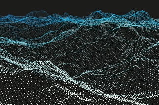
Nanotopography of an Atomic World
January 16, 2019 | Pennsylvania State UniversityEstimated reading time: 3 minutes
Physicists offer insights into the structure of atomically thin materials using nanoscale images of 2D membranes.
Nanoscale materials are at the forefront of solving some of the world’s biggest engineering challenges. With everything from super-light bicycles to quantum electronics made possible with nanotechnology, researchers are eager to tap into the vast potential of these materials.
But scaling things up from an atomic level is a monumental task, and making usable amounts of nanoscale materials continues to be a significant hurdle for materials scientists and engineers.
Now, researchers in Penn’s Department of Physics & Astronomy are paving the way for the future of nanomaterial applications by providing insights into how these thin 2D membranes form. The study from the lab of Marija Drndić, published in the journal Nano Letters, also offers a view of what these materials look like at the nanometer scale.
The study builds on previous work done by the Drndić lab and focuses on a “less attractive” form of 2D membranes. Most research in the field focuses on membranes that are comprised of a monolayer that is only one atom thick. In this study, the Drndić lab used membranes that have a mix of thicknesses. In some areas of the membrane, the thickness is only one or two atoms, while in others membranes are about 10 atoms thick.
These membranes are considered “less attractive” because they may not be ideal for applications such as electronics. However, these membranes are strong, versatile, and much easier to make in the lab. “This additional robustness can be used for applications like desalination or gas transport,” says Priyanka Thiruraman, a graduate student involved with the study.
Making this kind of porous 2D membrane requires three steps. The first is to grow the membranes on sheets of molybdenum foil by heating them to 800°C (about 1470°F) in a chamber with sulfur vapor. This process creates the 2D membrane, which is made of molybdenum bound with sulfur.
The second step is to add atomic-scale holes to the membrane using a process called acid etching. Both the growing and the etching can be finished in a single day. “You don’t need any special chemicals to make these membranes,” says Paul Masih Das, a graduate student who was the lead author of this study. “You could even make them in your basement.”
The third step is where this work goes from something you could do in your basement to cutting-edge physics research. It’s also what makes this particular study so impactful.
Using a scanning transmission electron microscope, Masih Das was able to take pictures of these membranes at an atomic scale, bringing to life the shape of these membranes through “nanotopography.” The images show the layout of individual atoms within the membrane and reveal patterns that resemble a map of atomic hills and valleys. “This level of structure, where we can see the individual atoms of these multilayer molybdenum disulfide membranes, hasn’t been seen in the related literature before,” says Drndić.
Masih Das said that these results were unexpected; they thought they would find a structure that was more uniform and grid-like. It’s unexpected results like this that drive the Drndić lab to keep exploring the potential of how these “less attractive” materials could be used in the future.
“The idea of desalination came naturally. It’s not that we planned it; it was just that for the holes that we were making for DNA sequencing applications we noticed that if they were smaller then we can filter ions. When we first published on that topic, there were not many papers at all out there. Now, all of a sudden, there are many more papers, and there’s more of a research community.”
The Drndić lab continues to study the fundamental nature of 2D membranes and other nanomaterials. “We let it grow naturally,” Drndić says about the work done in her lab. “If we see another opportunity, we might jump on it. It’s nice to have that kind of freedom, where you’re not under pressure to always justify the cost or the application. It’s nice to be able to just explore and to bump onto new things.”
Share on:


Testimonial
"Your magazines are a great platform for people to exchange knowledge. Thank you for the work that you do."
Simon Khesin - Schmoll MaschinenSuggested Items
ITW EAE Despatch Ovens Now Support ASTM 5423 Testing
10/15/2025 | ITW EAEAs the demand for high-performance electrical insulation materials continues to grow—driven by the rapid expansion of electric vehicles (EVs) and energy storage systems—thermal processing has become a critical step in material development.
Beyond Thermal Conductivity: Exploring Polymer-based TIM Strategies for High-power-density Electronics
10/13/2025 | Padmanabha Shakthivelu and Nico Bruijnis, MacDermid Alpha Electronics SolutionsAs power density and thermal loads continue to increase, effective thermal management becomes increasingly important. Rapid and efficient heat transfer from power semiconductor chip packages is essential for achieving optimal performance and ensuring long-term reliability of temperature-sensitive components. This is particularly crucial in power systems that support advanced applications such as green energy generation, electric vehicles, aerospace, and defense, along with high-speed computing for data centers and artificial intelligence (AI).
Is Glass Finally Coming of Age?
10/13/2025 | Nolan Johnson, I-Connect007Substrates, by definition, form the base of all electronic devices. Whether discussing silicon wafers for semiconductors, glass-and-epoxy materials in printed circuits, or the base of choice for interposers, all these materials function as substrates. While other substrates have come and gone, silicon and FR-4 have remained the de facto standards for the industry.
Creative Materials to Showcase Innovative Functional Inks for Medical Devices at COMPAMED 2025
10/09/2025 | Creative Materials, Inc.Creative Materials, a leading manufacturer of high-performance functional inks and coatings, is pleased to announce its participation in COMPAMED 2025, taking place November 17–20 in Düsseldorf, Germany.
Jiva Leading the Charge Toward Sustainable Innovation
09/30/2025 | Marcy LaRont, PCB007 MagazineEnvironmental sustainability in business—product circularity—is a high priority these days. “Circularity,” the term meant to replace “recycling,” in its simplest definition, describes a full circle life for electronic products and all their elements. The result is re-use or a near-complete reintroduction of the base materials back into the supply chain, leaving very little left for waste. For what cannot be reused productively, the ultimate hope is to have better, less harmful means of disposal and/or materials that can seamlessly and harmlessly decompose and integrate back into the natural environment. That is where Jiva and Soluboard come in.