


 The Marketing Minute: Marketing With Layers
 The Right Approach: Electro-Tek—A Williams Family Legacy, Part 1
 It’s Only Common Sense: If You’re Not Differentiated, You’re Dead


Imec and CARDIS Partners Develop Unique Photonic-Based Medical Device
January 17, 2019 | ImecEstimated reading time: 3 minutes
Imec, the world-leading research and innovation hub in nanoelectronics and digital technology and Ghent University, together with Medtronic and other CARDIS project partners, have developed a prototype medical device based on silicon photonics for the screening of arterial stiffness and for the diagnosis of cardiovascular diseases such as arterial stenosis and heart failure. A clinical feasibility study with 100 patients has been successfully completed by INSERM at the Georges Pompidou European Hospital in Paris, France.
Cardiovascular disease (CVD) is among the leading causes of death globally. Early identification of individuals at risk allows for early intervention to halt or reverse the pathological process. Assessment of arterial stiffness by measurement of aortic pulse wave velocity (aPWV) is included in the latest guidelines for CVD risk prediction and it is a key marker for hypertension. However, no tools are available today to easily screen a large number of patients for arterial stiffness at a GP’s office. As a consequence, many individuals remain undiagnosed.
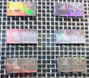
In the Horizon 2020 project CARDIS, imec, Medtronic, and 7 other partners, have developed a prototype mobile, low-cost, point-of-care screening device for CVD. The device aims for measurement in a fast, reproducible and reliable way with minimal physical contact with the patient and minimal skills from the operator. The operating principle of the device is Laser Doppler Vibrometry (LDV), in which a very low-power laser is directed towards the skin overlying an artery. The skin’s vibration amplitude and frequency, resulting from the heart beat, are extracted from the Doppler shift of the reflected beam. The device includes two rows of six beams, thereby scanning multiple points on the skin above the artery in parallel.
At the heart of the system is a silicon photonics chip containing the optical functionality of the multi-beam LDV device. The CARDIS chip was designed by the Photonics Research Group, an imec laboratory at Ghent University, and prototyped through imec’s silicon photonics technology platform iSiPP50G, and has been implemented using advanced optical packaging approaches developed at the Tyndall National Institute in Ireland. The system has then been integrated into a handheld device and validated for human use by Medtronic.
A clinical feasibility study at the Georges Pompidou European Hospital in Paris has collected a substantial clinical dataset, both from healthy subjects as well as from patients with cardiovascular conditions. The quality of the device readings was found to be very good and adequate measurement results could be obtained in all subjects. Also, the measurement data and variability within sessions were in line with data and variability acquired by reference techniques. A full dataset is now available and in-depth analysis will be performed both at INSERM and at the biomedical engineering department of Ghent University with the support of Medtronic. Moreover, further clinical feasibility studies are planned in the Academic Hospital of Maastricht (The Netherlands).
“The CARDIS device was well accepted by all patients, and it was considered useful and well tolerated,” states Dr. Pierre Boutouyrie, the cardiologist in charge of the feasibility study. “Feasibility of signal acquisition is excellent since a useful signal was acquired in 100% of the patients. Tolerance was excellent too, the time to get useful signals was less than 10 min, and patients barely noticed that a measurement was performed.”
Roel Baets, head of the Photonics Research Group (imec/UGent), concludes: “Silicon photonics is a powerful technology that combines the unique sensing capabilities of photonics with the low-cost and miniaturization capabilities of silicon semiconductor technology. It’s exciting to know that our silicon photonic chip and prototype medical device hold the promise to change the lives of so many patients with cardiovascular diseases.”
In a next step, a small series of the device will be produced to perform a clinical feasibility study on a larger group of patients and over a longer period of time. If this feasibility study demonstrates the ability of the technology to detect cardiovascular diseases at an early stage, high volume production can be initiated. One of the benefits of the silicon photonics technology is that at high volumes, the chip can be produced at low cost.
Share on:


Testimonial
"Your magazines are a great platform for people to exchange knowledge. Thank you for the work that you do."
Simon Khesin - Schmoll MaschinenSuggested Items
China Expands Rare Earth Export Restrictions, Tightening Grip on Global Supply Chains
10/16/2025 | I-Connect007 Editorial TeamChina sharply expanded its rare earth export restrictions on Oct. 9, adding additional elements and refining technologies to its control list while imposing stricter rules on foreign users in the defense and semiconductor industries.
SAMI Advanced Electronics Company Launches “Remal” Computer Manufacturing Project in Partnership with HP and Foxconn
10/15/2025 | SAMI-AECSAMI Advanced Electronics Company (SAMI-AEC), a wholly owned subsidiary of Saudi Arabian Military Industries (SAMI), proudly announced the launch of the “Remal” project for computer manufacturing, in strategic partnership with HP and Foxconn.
The Right Approach: Electro-Tek—A Williams Family Legacy, Part 1
10/15/2025 | Steve Williams -- Column: The Right ApproachThere is no bronze bust in the lobby or portrait in the conference room of Electro-Tek's founder—my Dad, Charles “Chuck” Williams—so with the facility closing last year after 56 years, I feel it is time to tell the story. Chuck Williams founded Electro-Tek in 1968 in our basement, eventually moving into the second floor of an old 1913 building in downtown Milwaukee that is still standing (the first of three eventual facilities).
LPKF Joins productronica’s 50th Anniversary, Showcasing Laser Technology for Electronics Manufacturing
10/10/2025 | LPKF Laser & ElectronicsLPKF Laser & Electronics invites visitors to productronica 2025 in Munich from November 18 to 21. At booth 305 in hall B2, the company will present its portfolio of modern laser technologies for the electronics industry live – from prototyping systems and high-performance depaneling to laser plastic welding for electronic housings and thin glass processing for advanced packaging.
Marco Pieters Appointed ASML Chief Technology Officer
10/09/2025 | ASMLASML Holding NV (ASML) announced the appointment of Marco Pieters as Executive Vice President and Chief Technology Officer, reporting to President and Chief Executive Officer, Christophe Fouquet.