


 The Marketing Minute: Marketing With Layers
 The Right Approach: Electro-Tek—A Williams Family Legacy, Part 1
 It’s Only Common Sense: If You’re Not Differentiated, You’re Dead


Creating a Roadmap for 2D Materials
January 18, 2019 | Pennsylvania State UniversityEstimated reading time: 4 minutes
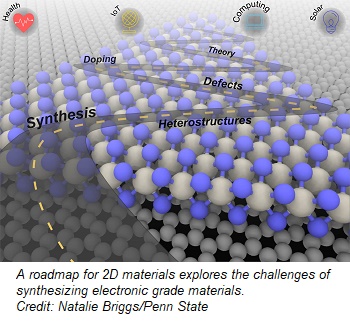
The rapid growth of research on 2D materials – materials such as graphene and others that are a single or few atoms thick – is fueled by the hope of developing better performing sensors for health and environment, more economical solar energy, and higher performing and more energy efficient electronics than is possible with current silicon electronics.
The rapid growth of research on 2D materials – materials such as graphene and others that are a single or few atoms thick – is fueled by the hope of developing better performing sensors for health and environment, more economical solar energy, and higher performing and more energy efficient electronics than is possible with current silicon electronics.
Technical roadmaps, such as the International Technology Roadmap for Semiconductors (ITRS), first published in 1998, serve as guides for future advances in a particular field and provide a means for organizations to plan for investments in new technology.
An invited article in the December online edition of the journal 2D Materials provides a roadmap for the synthesis of electronic-grade two-dimensional materials for future electronic and sensing applications. Led by Penn State, with contributions from five additional universities and national laboratories, the roadmap addresses the grand challenges in 2D materials with useful electronic or photonic properties, and the outlook for U.S. advances in the field.
“This article is a review of where we currently are in regard to the synthesis of 2D materials and our thoughts on the top research priorities that need to be addressed to achieve electronic grade 2D materials,” said Joshua Robinson, associate professor of materials science and engineering, whose Ph.D. students Natalie Briggs and Shruti Subramanian are co-lead authors on the report titled “A Roadmap for Electronic Grade 2-Dimensional Materials,” published online today, Jan. 17.
“2D materials are touted to be revolutionary for a variety of technologies, assuming the materials are perfect,” he said. “But that’s never the case – we have a long way to go before the materials are perfect. Our hope is that the roadmap provides a guide to get us there. Once that happens, the technology can really take off.”
The authors divided the paper into four parts: Grand Challenges, which are the technology drivers, such as the internet of things; Synthesis, the techniques and theories required to grow close to perfect 2D materials; Materials Engineering, which is fine tuning the properties of 2D and composite materials; and finally, Outlook, which is the future of electronic devices when silicon technology reaches an inevitable roadblock.
“To put our roadmap together, we reached out to experts in various subfields, such as different synthesis approaches, defect engineering and computational theory,” said Briggs of the two-year project. “We asked them to talk about the key fundamental challenges and the steps required to address these challenges in their area of expertise.”
Robinson added, “This is the first roadmap focused on 2D synthesis for electronic applications and there are still a lot of open questions. We want to bring some of those topics into the light.”
A list of the twenty authors and their affiliations can be found online in the open access article in 2D Materials.
roadmaps, such as the International Technology Roadmap for Semiconductors (ITRS), first published in 1998, serve as guides for future advances in a particular field and provide a means for organizations to plan for investments in new technology.
An invited article in the December online edition of the journal 2D Materials provides a roadmap for the synthesis of electronic-grade two-dimensional materials for future electronic and sensing applications. Led by Penn State, with contributions from five additional universities and national laboratories, the roadmap addresses the grand challenges in 2D materials with useful electronic or photonic properties, and the outlook for U.S. advances in the field.
“This article is a review of where we currently are in regard to the synthesis of 2D materials and our thoughts on the top research priorities that need to be addressed to achieve electronic grade 2D materials,” said Joshua Robinson, associate professor of materials science and engineering, whose Ph.D. students Natalie Briggs and Shruti Subramanian are co-lead authors on the report titled “A Roadmap for Electronic Grade 2-Dimensional Materials”.
“2D materials are touted to be revolutionary for a variety of technologies, assuming the materials are perfect,” he said. “But that’s never the case – we have a long way to go before the materials are perfect. Our hope is that the roadmap provides a guide to get us there. Once that happens, the technology can really take off.”
The authors divided the paper into four parts: Grand Challenges, which are the technology drivers, such as the internet of things; Synthesis, the techniques and theories required to grow close to perfect 2D materials; Materials Engineering, which is fine tuning the properties of 2D and composite materials; and finally, Outlook, which is the future of electronic devices when silicon technology reaches an inevitable roadblock.
“To put our roadmap together, we reached out to experts in various subfields, such as different synthesis approaches, defect engineering and computational theory,” said Briggs of the two-year project. “We asked them to talk about the key fundamental challenges and the steps required to address these challenges in their area of expertise.”
Robinson added, “This is the first roadmap focused on 2D synthesis for electronic applications and there are still a lot of open questions. We want to bring some of those topics into the light.”
A list of the twenty authors and their affiliations can be found online in the open access article in 2D Materials.
Share on:


Testimonial
"The I-Connect007 team is outstanding—kind, responsive, and a true marketing partner. Their design team created fresh, eye-catching ads, and their editorial support polished our content to let our brand shine. Thank you all! "
Sweeney Ng - CEE PCBSuggested Items
China Expands Rare Earth Export Restrictions, Tightening Grip on Global Supply Chains
10/16/2025 | I-Connect007 Editorial TeamChina sharply expanded its rare earth export restrictions on Oct. 9, adding additional elements and refining technologies to its control list while imposing stricter rules on foreign users in the defense and semiconductor industries.
SAMI Advanced Electronics Company Launches “Remal” Computer Manufacturing Project in Partnership with HP and Foxconn
10/15/2025 | SAMI-AECSAMI Advanced Electronics Company (SAMI-AEC), a wholly owned subsidiary of Saudi Arabian Military Industries (SAMI), proudly announced the launch of the “Remal” project for computer manufacturing, in strategic partnership with HP and Foxconn.
The Right Approach: Electro-Tek—A Williams Family Legacy, Part 1
10/15/2025 | Steve Williams -- Column: The Right ApproachThere is no bronze bust in the lobby or portrait in the conference room of Electro-Tek's founder—my Dad, Charles “Chuck” Williams—so with the facility closing last year after 56 years, I feel it is time to tell the story. Chuck Williams founded Electro-Tek in 1968 in our basement, eventually moving into the second floor of an old 1913 building in downtown Milwaukee that is still standing (the first of three eventual facilities).
LPKF Joins productronica’s 50th Anniversary, Showcasing Laser Technology for Electronics Manufacturing
10/10/2025 | LPKF Laser & ElectronicsLPKF Laser & Electronics invites visitors to productronica 2025 in Munich from November 18 to 21. At booth 305 in hall B2, the company will present its portfolio of modern laser technologies for the electronics industry live – from prototyping systems and high-performance depaneling to laser plastic welding for electronic housings and thin glass processing for advanced packaging.
Marco Pieters Appointed ASML Chief Technology Officer
10/09/2025 | ASMLASML Holding NV (ASML) announced the appointment of Marco Pieters as Executive Vice President and Chief Technology Officer, reporting to President and Chief Executive Officer, Christophe Fouquet.