


 The Marketing Minute: Marketing With Layers
 The Right Approach: Electro-Tek—A Williams Family Legacy, Part 1
 It’s Only Common Sense: If You’re Not Differentiated, You’re Dead


Properties of ‘Wonder Material’ Graphene Change in Humid Conditions
January 22, 2019 | Queen Mary University of LondonEstimated reading time: 2 minutes
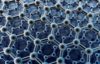
The ‘wonder material’, which is made from carbon and was discovered in 2004, is hailed for many of its extraordinary characteristics including being stronger than steel, more conductive than copper, light, flexible and transparent.
This study, published in the journal Physical Review B, shows that in bi-layer graphene, which is two sheets of one atom thick carbon stacked together, water seeps between the layers in a humid environment.
The properties of graphene significantly depend on how these carbon layers interact with each other and when water enters in between it can modify the interaction.
The researchers found the water forms an atomically thin layer at 22% relative humidity and separates graphene layers at over 50% relative humidity.
This suggests that layered graphene could exhibit very different properties in a humid place such as Manchester, UK, where average relative humidity is over 80% every month of the year, compared to a dry place such as Tucson, Arizona, where relative humidity is 13% on afternoons in May but rises to 65% on January mornings. So, in Tucson the properties will vary according to the time of the year.
Graphene, both layered and single layer, potentially has a huge number of uses but the results of this study could impact how the material can be used in real-life applications.
Humidity Needs to be Recorded
Lead author Dr Yiwei Sun, from Queen Mary's School of Engineering and Materials Science, said: “The critical points, 22% and 50% relative humidity, are very common conditions in daily life and these points can be easily crossed. Hence, many of the extraordinary properties of graphene could be modified by water in between graphene layers.”
“Some graphene-based devices may function to their full capability in dry places while others may do so in humid places. We suggest all experiments on 2D materials should in future record the relative humidity,” he added.
The researchers suggest humidity is also likely to have an impact on other layered materials such as boron nitride (sheets made of boron and nitrogen) and Molybdenum disulphide (sheets made of molybdenum and sulphur).
The study was carried out because it was known that graphite, a material also made from carbon, loses its excellent lubricating ability in low humidity conditions, such as aboard aeroplanes at high altitude, which was reported during the Second World War, or in outer space, as reported by NASA in the 1970s.
It was believed that the water in between layers of graphite is crucial to its behaviour and now the same effect has been shown to affect layered graphene.
Share on:


Testimonial
"Our marketing partnership with I-Connect007 is already delivering. Just a day after our press release went live, we received a direct inquiry about our updated products!"
Rachael Temple - AlltematedSuggested Items
Episode 6 of Ultra HDI Podcast Series Explores Copper-filled Microvias in Advanced PCB Design and Fabrication
10/15/2025 | I-Connect007I-Connect007 has released Episode 6 of its acclaimed On the Line with... American Standard Circuits: Ultra High Density Interconnect (UHDI) podcast series. In this episode, “Copper Filling of Vias,” host Nolan Johnson once again welcomes John Johnson, Director of Quality and Advanced Technology at American Standard Circuits, for a deep dive into the pros and cons of copper plating microvias—from both the fabricator’s and designer’s perspectives.
Nolan’s Notes: Tariffs, Technologies, and Optimization
10/01/2025 | Nolan Johnson -- Column: Nolan's NotesLast month, SMT007 Magazine spotlighted India, and boy, did we pick a good time to do so. Tariff and trade news involving India was breaking like a storm surge. The U.S. tariffs shifted India from one of the most favorable trade agreements to the least favorable. Electronics continue to be exempt for the time being, but lest you think that we’re free and clear because we manufacture electronics, steel and aluminum are specifically called out at the 50% tariff levels.
MacDermid Alpha & Graphic PLC Lead UK’s First Horizontal Electroless Copper Installation
09/30/2025 | MacDermid Alpha & Graphic PLCMacDermid Alpha Electronics Solutions, a leading supplier of integrated materials and chemistries to the electronics industry, is proud to support Graphic PLC, a Somacis company, with the installation of the first horizontal electroless copper metallization process in the UK.
Electrodeposited Copper Foils Market to Grow by $11.7 Billion Over 2025-2032
09/18/2025 | Globe NewswireThe global electrodeposited copper foils market is poised for dynamic growth, driven by the rising adoption in advanced electronics and renewable energy storage solutions.
MacDermid Alpha Showcases Advanced Interconnect Solutions at PCIM Asia 2025
09/18/2025 | MacDermid Alpha Electronics SolutionsMacDermid Alpha Electronic Solutions, a global leader in materials for power electronics and semiconductor assembly, will showcase its latest interconnect innovations in electronic interconnect materials at PCIM Asia 2025, held from September 24 to 26 at the Shanghai New International Expo Centre, Booth N5-E30