


 The Marketing Minute: Marketing With Layers
 The Right Approach: Electro-Tek—A Williams Family Legacy, Part 1
 It’s Only Common Sense: If You’re Not Differentiated, You’re Dead


We Need Smart Combinations for Next Generation Photonics
January 22, 2019 | University of TwenteEstimated reading time: 2 minutes
Photonics and radio signals join forces for high-speed mobile data communication, like in 5G communications. At the same time, the applications of ‘integrated microwave photonics’ go way beyond telecom. This progress often comes from directions you would not expect in the first place. University of Twente researcher David Marpaung (MESA+ Insitute), for example, works on a combination of light and sound waves, enabling him to design high-quality filters. In a review paper in Nature Photonics, he gives a vision on the next phase of photonic chips, for example in brain-inspired, ‘neuromorphic’ optical computing.
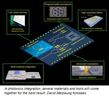
Soon, a single type of photonic chip—a chip that processes light instead of electrons—can’t do the job by its own, is David Marpaung’s expectation. The trend is: find smart combinations of materials and tools, then integrated microwave photonics can really make the difference. His own research is about the combination of light, radio frequency, and acoustic waves. Photonic chips will convert radio signals into light that works at much higher frequencies. In this way, a fast optical link is possible between two base stations for mobile wireless communication. At radio frequencies, however, very precise filtering is possible for selecting the specific part of the crowded radio bands. As soon as the radio signal is converted into light, filtering is more complicated as light, in fact, travels too fast. There, acoustic waves come in: they are capable of slowing down the light, so filters can be designed in the optical domain, that are sufficiently selective. This is called ‘stimulated Brillouin scattering’, for which Marpaung received a Dutch NWO-vidi research grant.
In photonics integration, several materials and tools will come together for the best result, David Marpaung foresees.
Multi-Material
The paper David Marpaung wrote together with experts Jianping Yao of the University of Ottawa and Jose Campany of the University of Valencia, is a broad vision of the future and a plea for finding creative combinations. At this moment, the three main materials for photonics are silicon nitride, indium phosphide and silicon-on-insulator, each of them with its specific advantages. The future is about ‘hybrid systems’ employing combinations of materials and technologies: recent UT work already shows integrating photonics and CMOS electronics, which has the advantage of a mature and very large-scale production technology. Solutions also come from micromechanics. Instead of employing several lasers for one photonics chip, consuming a lot of space and energy, a comb-like structure of ‘microresonators’ can do the job.
Reconfigurable
Thanks to these developments, in which several disciplines meet, microwave photonics can be developed way beyond its origin of telecom and signal processing. Using basic photonics components like ‘Mach-Zehnder interferometers’, enabling logic operations with light, very flexible photonic processors can now be developed, that can be reconfigured for specific applications. Marpaung currently develops such advanced technologies with University of Twente spinoff LioniX. The University of Twente has a cluster of researchers working in photonics, called Applied Nanophotonics, part of the MESA+ Institute.
Spikes
New application areas include optical quantum computing and brain-inspired, ‘neuromorphic’ computing: can we translate the ‘spikes’ in our brain, neurons that ‘fire’, into a photonic processor, thus mimicking how our brain works? Again, combination of technologies and materials will be key to success.
Share on:


Testimonial
"We’re proud to call I-Connect007 a trusted partner. Their innovative approach and industry insight made our podcast collaboration a success by connecting us with the right audience and delivering real results."
Julia McCaffrey - NCAB GroupSuggested Items
ITW EAE Despatch Ovens Now Support ASTM 5423 Testing
10/15/2025 | ITW EAEAs the demand for high-performance electrical insulation materials continues to grow—driven by the rapid expansion of electric vehicles (EVs) and energy storage systems—thermal processing has become a critical step in material development.
Beyond Thermal Conductivity: Exploring Polymer-based TIM Strategies for High-power-density Electronics
10/13/2025 | Padmanabha Shakthivelu and Nico Bruijnis, MacDermid Alpha Electronics SolutionsAs power density and thermal loads continue to increase, effective thermal management becomes increasingly important. Rapid and efficient heat transfer from power semiconductor chip packages is essential for achieving optimal performance and ensuring long-term reliability of temperature-sensitive components. This is particularly crucial in power systems that support advanced applications such as green energy generation, electric vehicles, aerospace, and defense, along with high-speed computing for data centers and artificial intelligence (AI).
Is Glass Finally Coming of Age?
10/13/2025 | Nolan Johnson, I-Connect007Substrates, by definition, form the base of all electronic devices. Whether discussing silicon wafers for semiconductors, glass-and-epoxy materials in printed circuits, or the base of choice for interposers, all these materials function as substrates. While other substrates have come and gone, silicon and FR-4 have remained the de facto standards for the industry.
Creative Materials to Showcase Innovative Functional Inks for Medical Devices at COMPAMED 2025
10/09/2025 | Creative Materials, Inc.Creative Materials, a leading manufacturer of high-performance functional inks and coatings, is pleased to announce its participation in COMPAMED 2025, taking place November 17–20 in Düsseldorf, Germany.
Jiva Leading the Charge Toward Sustainable Innovation
09/30/2025 | Marcy LaRont, PCB007 MagazineEnvironmental sustainability in business—product circularity—is a high priority these days. “Circularity,” the term meant to replace “recycling,” in its simplest definition, describes a full circle life for electronic products and all their elements. The result is re-use or a near-complete reintroduction of the base materials back into the supply chain, leaving very little left for waste. For what cannot be reused productively, the ultimate hope is to have better, less harmful means of disposal and/or materials that can seamlessly and harmlessly decompose and integrate back into the natural environment. That is where Jiva and Soluboard come in.